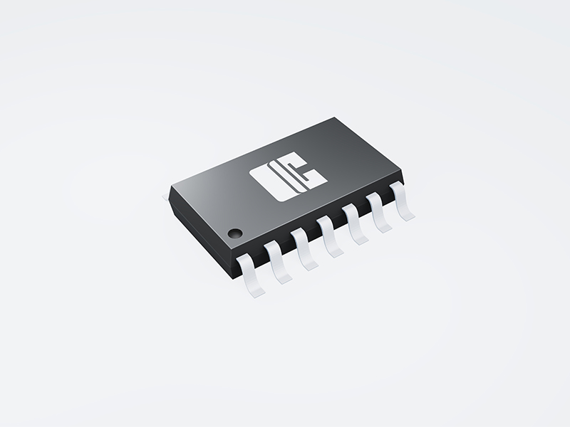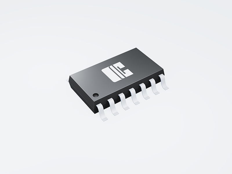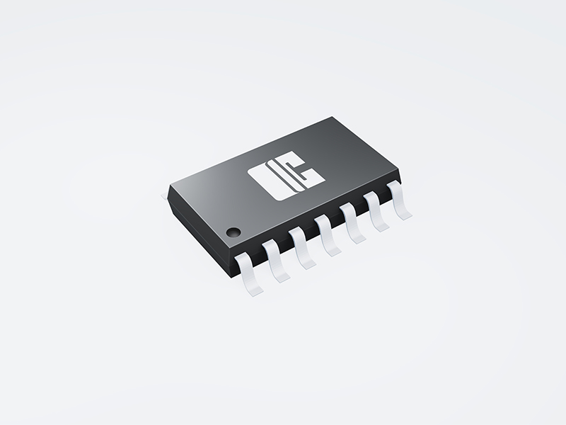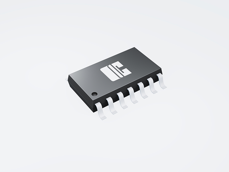
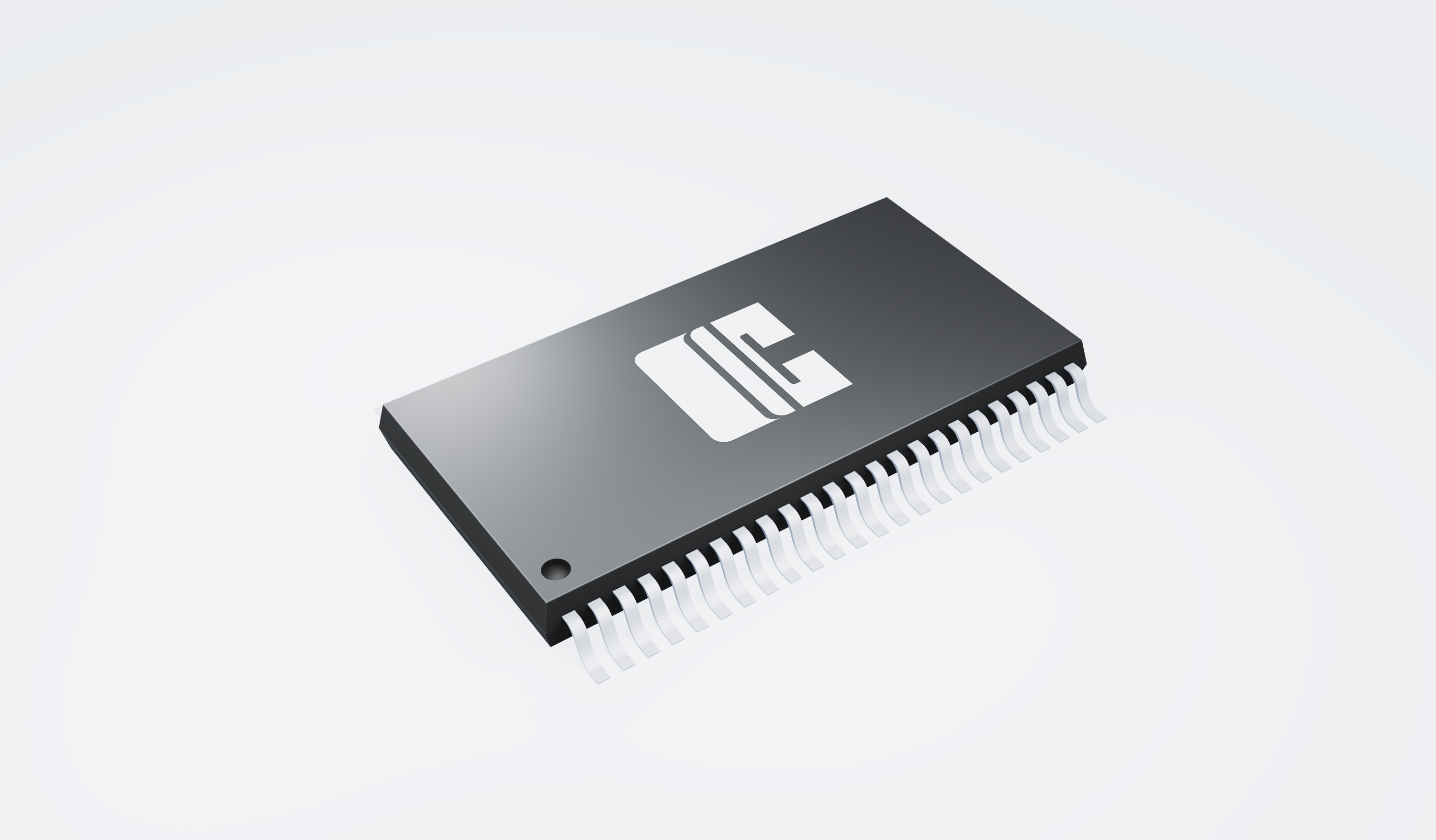
| The AiP74LVC/LVCH16245 are 16-bit transceivers featuring non-inverting 3-state bus compatible outputs in both send and receive directions. The device features two output enable (n ) inputs for easy cascading and two send/receive (nDIR) inputs for direction control. n controls the outputs so that the buses are effectively isolated. This device can be used as two 8-bit transceivers or one 16-bit transceiver. Inputs can be driven from either 3.3V or 5V devices. When disabled, up to 5.5V can be applied to the outputs. These features allow the use of these devices in mixed 3.3V and 5V applications. The AiP74LVCH16245 bus hold on data inputs eliminates the need for external pull-up resistors to hold unused inputs. |
PN :
AiP74LVCH16245Description :
16-bit Bus Transceiver; 3-stateVoltage Range :
1.2~5.5VNr of pins :
48Package :
TSSOP48| 5V tolerant inputs/outputs for interfacing with 5V logic Wide supply voltage range from 1.2V to 3.6V CMOS low power consumption MULTIBYTE flow-through standard pin-out architecture Low inductance multiple power and ground pins for minimum noise and ground bounce Direct interface with TTL levels High-impedance when VCC=0V All data inputs have bus hold (AiP74LVCH16245 only) Specified from -40℃ to +125℃ Packaging information: TSSOP48 |
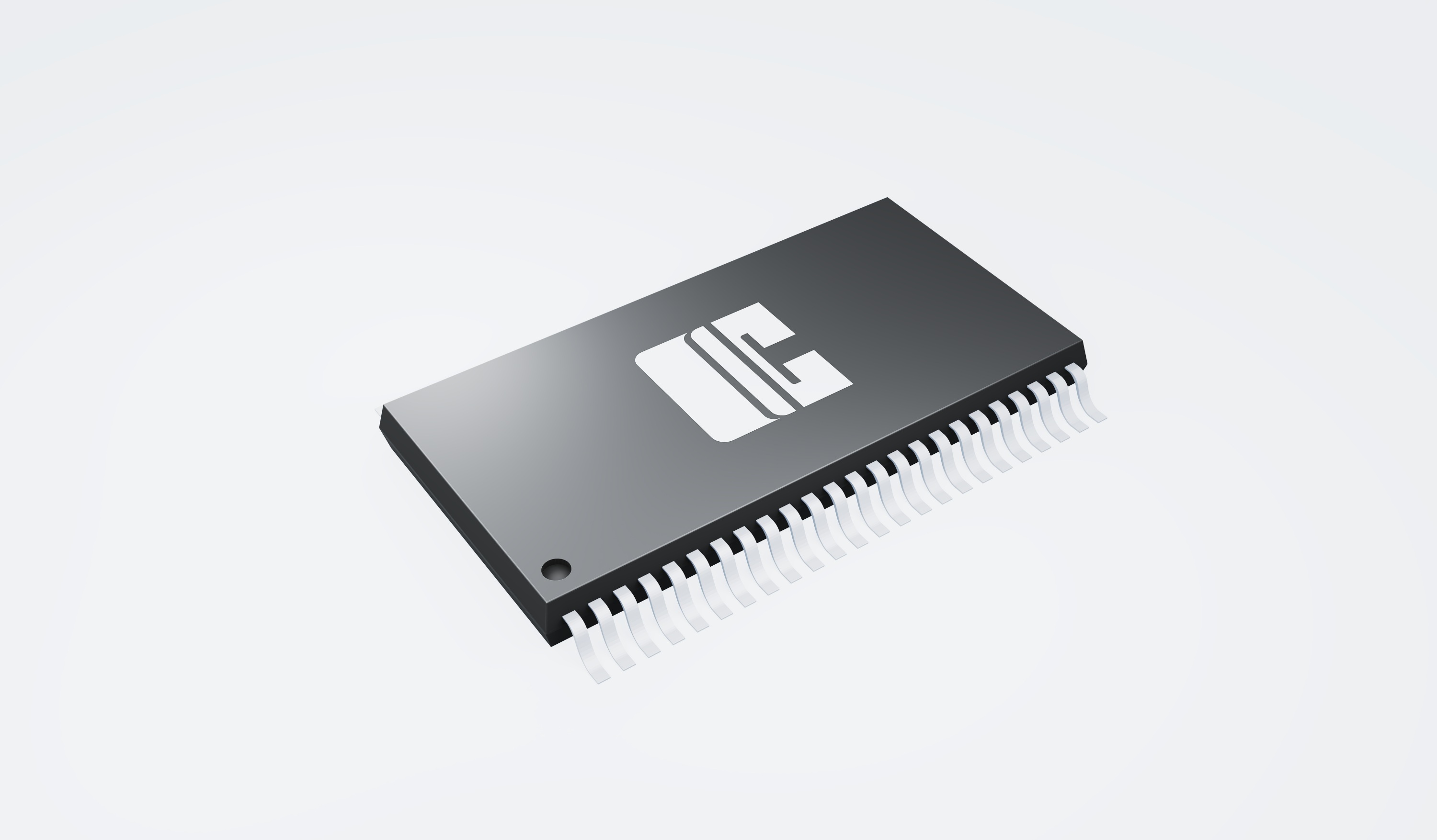
The AiP74AVC16T245 is a 16-bit transceiver with bidirectional level voltage translation and 3-state outputs.The device can be used as two 8-bit transceivers or as a 16-bit transceiver. It has dual supplies (VCC(A) and VCC(B)) for voltage translation and four 8-bit input-output ports (nAn and nBn) each with its own output enable (n ) and send/receive (nDIR) input for direction control. VCC(A) and VCC(B) can be independently supplied at any voltage between 0.8V and 3.6V making the device suitable for low voltage translation between any of the following voltages:0.8V,1.2V,1.5V,1.8V,2.5V and 3.3V. A HIGH on nDIR selects transmission from nAn to nBn while a LOW on nDIR selects transmission from nBn to nAn. A HIGH on n causes the outputs to assume a high-impedance OFF-stateThe device is fully specified for partial power-down applications using IOFF. The IOFF circuitry disables the output, preventing any damaging backflow current through the device when it is powered down. In suspend mode when either VCC(A) or VCC(B) are at GND level, both nAn and nBn are in the high-impedance OFF-state.
Details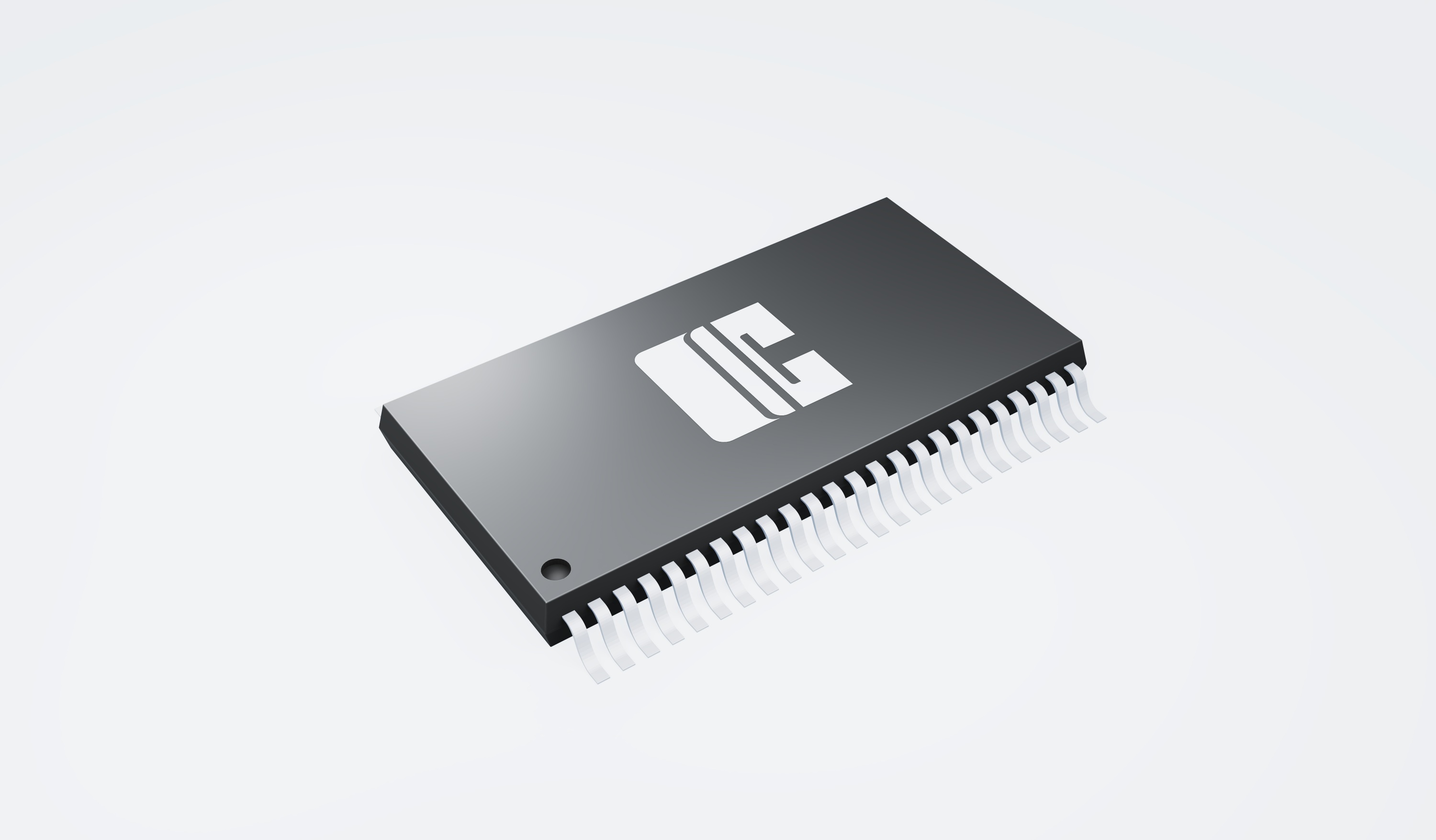
The AiP74AVC16T245 is a 16-bit transceiver with bidirectional level voltage translation and 3-state outputs.The device can be used as two 8-bit transceivers or as a 16-bit transceiver. It has dual supplies (VCC(A) and VCC(B)) for voltage translation and four 8-bit input-output ports (nAn and nBn) each with its own output enable (n ) and send/receive (nDIR) input for direction control. VCC(A) and VCC(B) can be independently supplied at any voltage between 0.8V and 3.6V making the device suitable for low voltage translation between any of the following voltages:0.8V,1.2V,1.5V,1.8V,2.5V and 3.3V. A HIGH on nDIR selects transmission from nAn to nBn while a LOW on nDIR selects transmission from nBn to nAn. A HIGH on n causes the outputs to assume a high-impedance OFF-stateThe device is fully specified for partial power-down applications using IOFF. The IOFF circuitry disables the output, preventing any damaging backflow current through the device when it is powered down. In suspend mode when either VCC(A) or VCC(B) are at GND level, both nAn and nBn are in the high-impedance OFF-state.
Details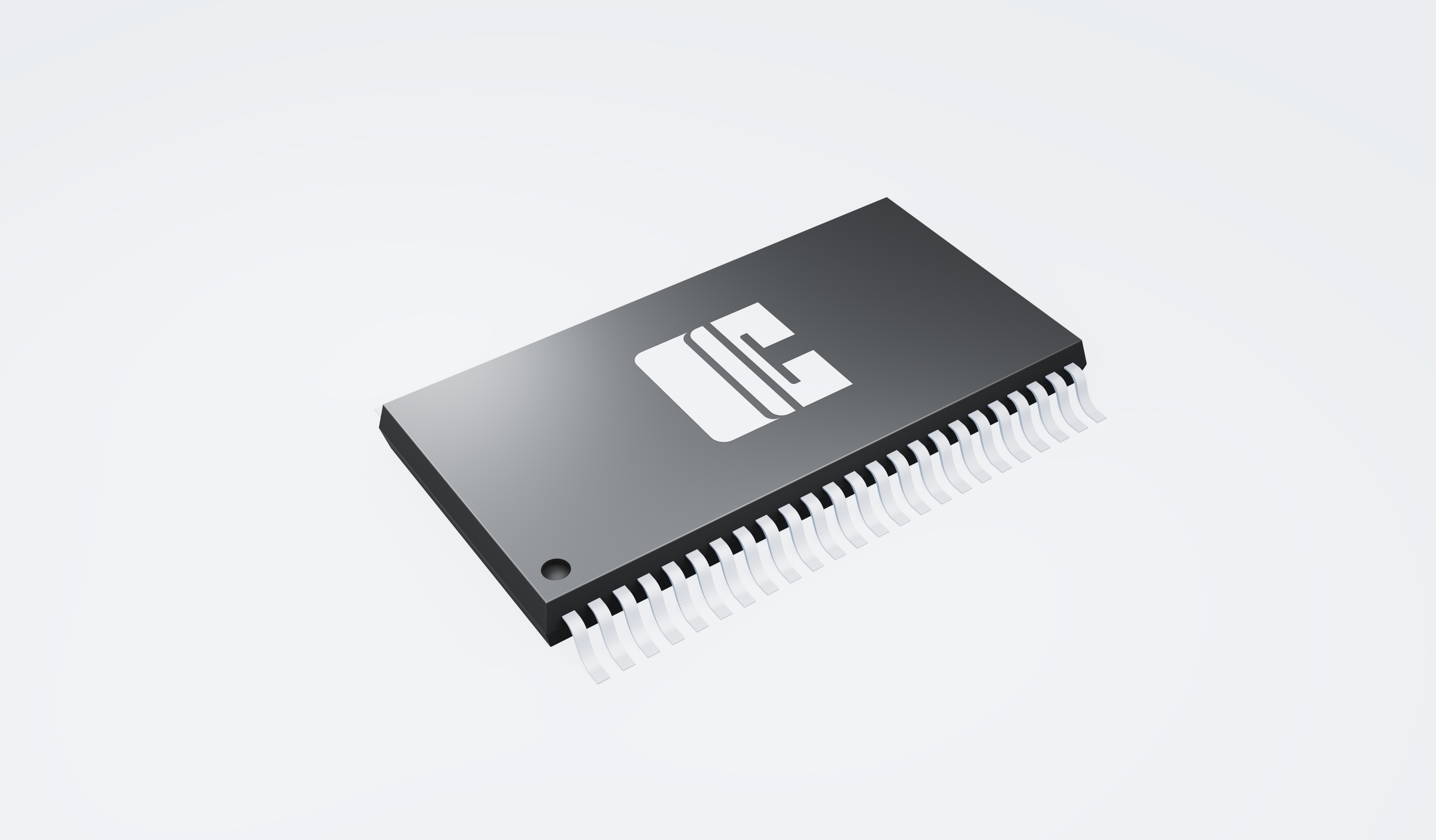
The AiP74AVC16245 is a 16-bit transceiver featuring non-inverting 3-state bus compatible outputs in both send and receive directions.
Details
The AiP74AUP1G00 provides the single 2-input NAND function. This device ensures a very low static and dynamic power consumption across the entire VCC range from 0.8V to 3.6V.
Details
The AiP74AUP1G00 provides the single 2-input NAND function. This device ensures a very low static and dynamic power consumption across the entire VCC range from 0.8V to 3.6V.
Details
The AiP74AUP1G04 provides the single inverting buffer.This device ensures a very low static and dynamic power consumption across the entire VCC range from 0.8V to 3.6V.
Details
The AiP74AUP1GU04 provides the single unbuffered inverting gate.This device ensures a very low static and dynamic power consumption across the entire VCC range from 0.8V to 3.6V.
Details
The AiP74AUP1G06 provides the single inverting buffer with open-drain output. This device ensures a very low static and dynamic power consumption across the entire VCC range from 0.8V to 3.6V.
Details
The AiP74AUP1G0832 provides the Boolean function: Y=(A×B)+C. The user can choose the logic fuctions OR, AND and AND-OR. This device ensures a very low static and dynamic power consumption across the entire VCC range from 0.8V to 3.6V.
Details
The AiP74AUP1G09 provides the single 2-input AND gate with an open-drain output. This device ensures a very low static and dynamic power consumption across the entire VCC range from 0.8V to 3.6V.
Details
The AiP74AUP1G11 provides the single 3-input AND function. This device ensures a very low static and dynamic power consumption across the entire VCC range from 0.8V to 3.6V.
Details
The AiP74AUP1G17 provides the single Schmitt trigger buffer.This device ensures a very low static and dynamic power consumption across the entire VCC range from 0.8V to 3.6V.
Details
The AiP74AUP1G34 provides two low-power, low-voltage buffers. This device ensures a very low static and dynamic power consumption across the entire VCC range from 0.8V to 3.6V.
Details
The AiP74AUP1G38 provides the single 2-input NAND gate with open-drain output. This device ensures a very low static and dynamic power consumption across the entire VCC range from 0.8V to 3.6V.
Details
The AiP74AUP1G57 provides configurable multiple functions. This device ensures a very low static and dynamic power consumption across the entire VCC range from 0.8V to 3.6V.
Details
The AiP74AUP1G58 provides configurable multiple functions. This device ensures a very low static and dynamic power consumption across the entire VCC range from 0.8V to 3.6V.
Details
The AiP74AUP1G79 provides the single positive-edge triggered D-type flip-flop. This device ensures a very low static and dynamic power consumption across the entire VCC range from 0.8V to 3.6V.
Details
The AiP74AUP1G86 provides the single 2-input EXCLUSIVE-OR gate function. This device ensures a very low static and dynamic power consumption across the entire VCC range from 0.8V to 3.6V.
Details
The AiP74AUP1G132 provides the single 2-input NAND Schmitt trigger.This device ensures a very low static and dynamic power consumption across the entire VCC range from 0.8V to 3.6V.
Details
The AiP74AUP1G332 provides a single 3-input OR gate. This device ensures a very low static and dynamic power consumption across the entire VCC range from 0.8V to 3.6V.
Details
The AiP74AUP1G373 provides the single D-type transparent latch 3-state output. This device ensures a very low static and dynamic power consumption across the entire VCC range from 0.8V to 3.6V.
Details
The AiP74AUP2G00 provides the dual the dual 2-input AND function. This device ensures a very low static and dynamic power consumption across the entire VCC range from 0.8V to 3.6V.
Details
The AiP74AUP2G02 provides a dual 2-input NOR function which accept standard input signals. This device ensures a very low static and dynamic power consumption across the entire VCC range from 0.8V to 3.6V.
Details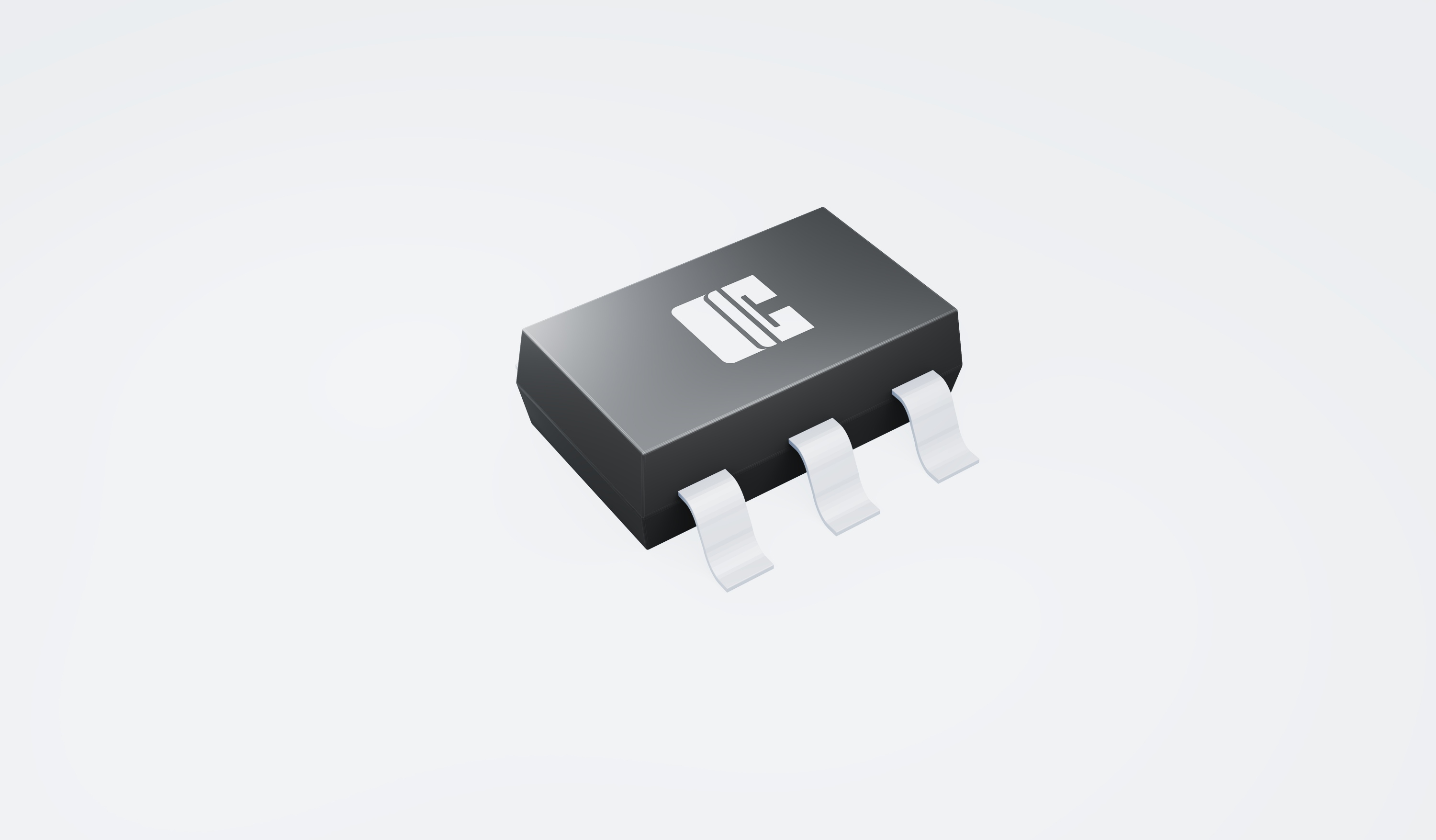
The AiP74AUP2G04 provides two inverting buffers.This device ensures a very low static and dynamic power consumption across the entire VCC range from 0.8V to 3.6V.
Details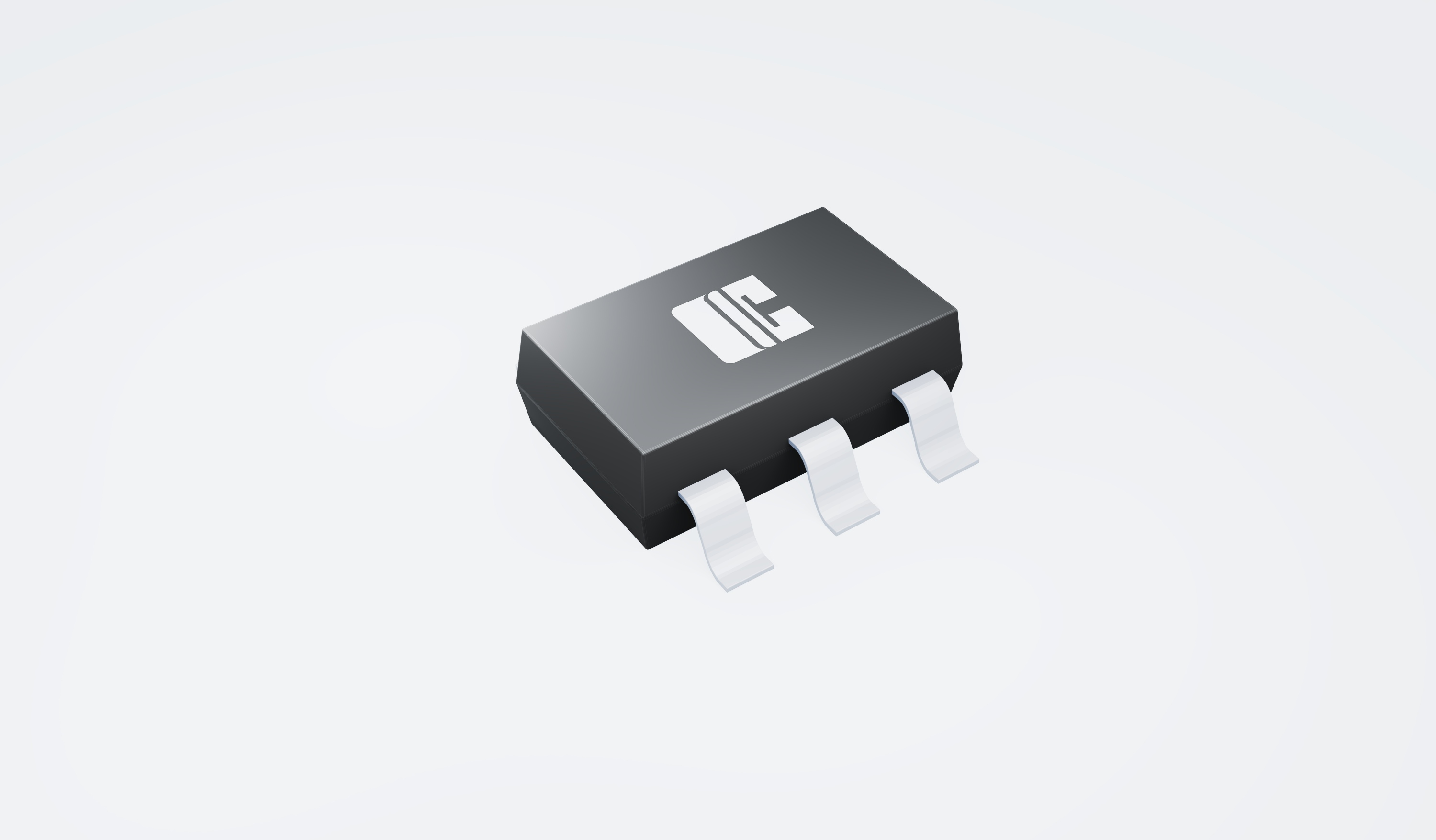
The AiP74AUP2GU04 provides two unbuffered inverting gates. This device ensures a very low static and dynamic power consumption across the entire VCC range from 0.8V to 3.6V
Details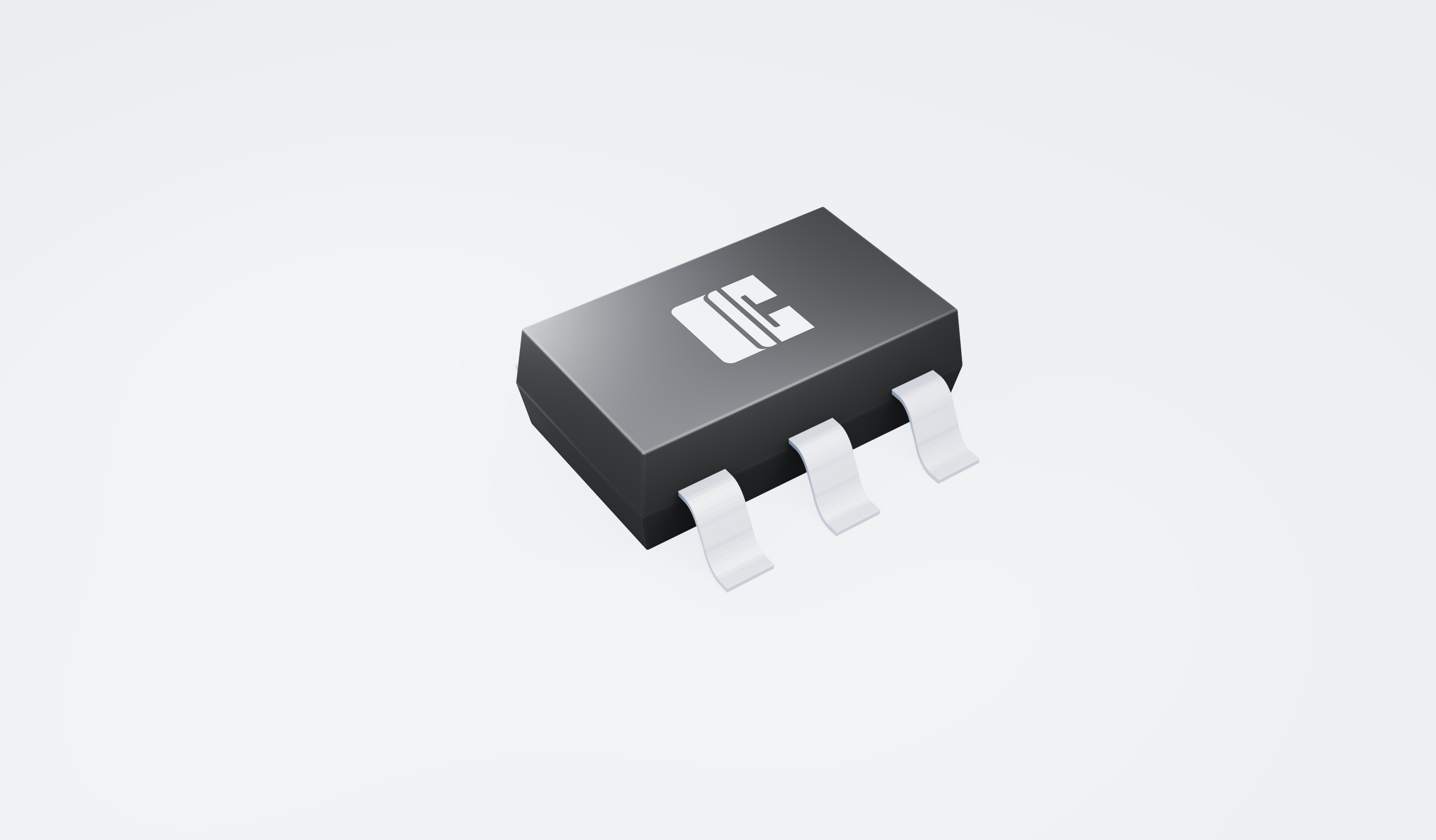
The AiP74AUP2G06 provides two inverting buffers with open-drain output. This device ensures a very low static and dynamic power consumption across the entire VCC range from 0.8V to 3.6V.
Details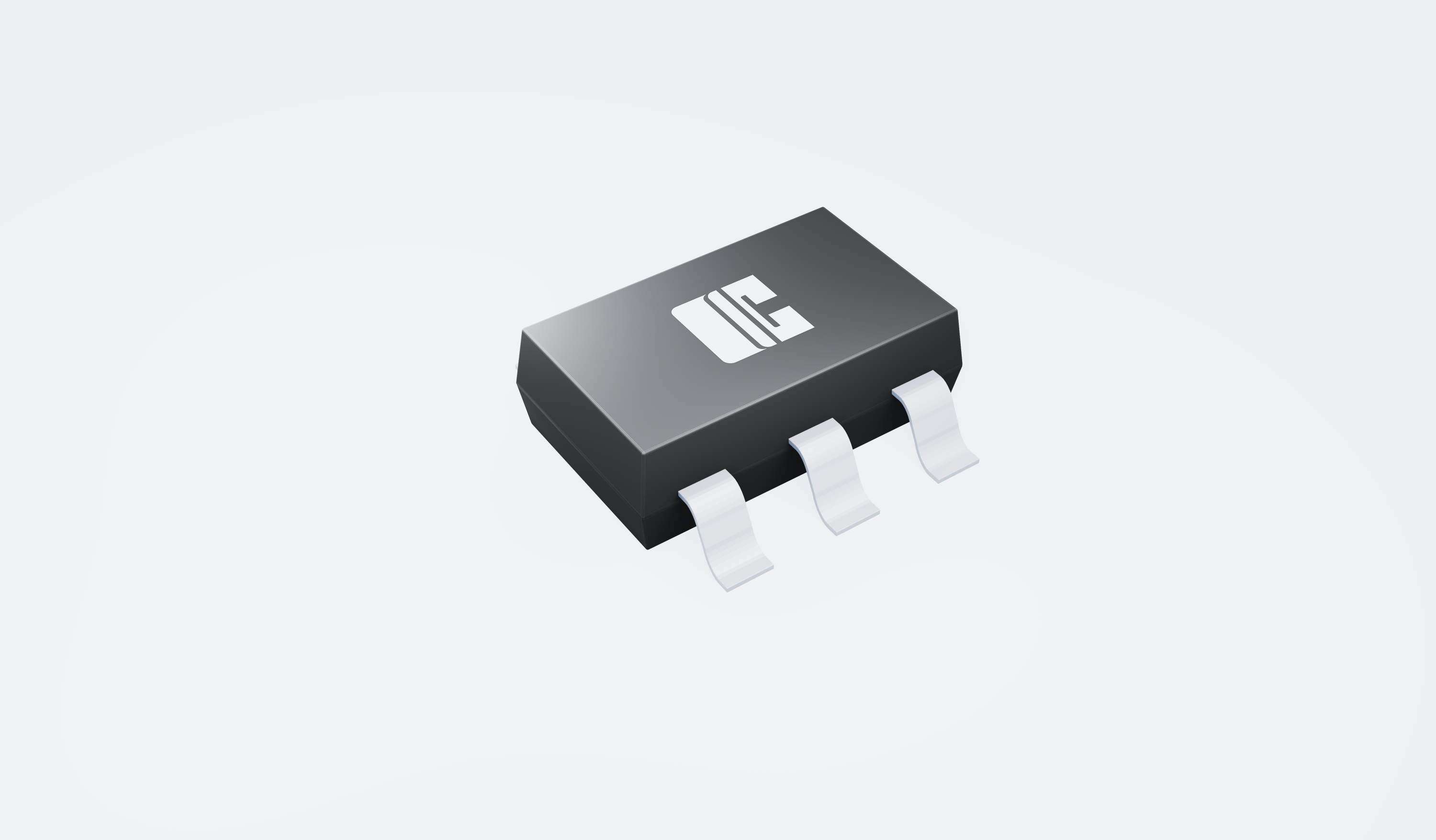
The AiP74AUP2G0604 provides a single inverting buffer with open-drain output and a single inverter which accept standard input signals.This device ensures a very low static and dynamic power consumption across the entire VCC range from 0.8V to 3.6V.
Details
The AiP74AUP2G07 provides two non-inverting buffer with open-drain output. This device ensures a very low static and dynamic power consumption across the entire VCC range from 0.8V to 3.6V.
Details
The AiP74AUP2G08 provides the dual the dual 2-input AND function.This device ensures a very low static and dynamic power consumption across the entire VCC range from 0.8V to 3.6V.
Details
The AiP74AUP2G09 provides a dual 2-input AND gate with an open-drain output. This device ensures a very low static and dynamic power consumption across the entire VCC range from 0.8V to 3.6V.
Details-177968936994yogwfur0.jpg)
The AiP74LVC08 provides four 2-input AND gates. Inputs can be driven from either 3.3V or 5V devices. This feature allows the use of these devices as translators in mixed 3.3V and 5V applications.
Details-1779689603FtroEi4lar.jpg)
The AiP74LV14 is a low-voltage Si-gate CMOS device that is pin and function compatible with AiP74HC14 and AiP74HCT14. The AiP74LV14 provides six inverting buffers with Schmitt-trigger input. It is capable of transforming slowly-changing input signals into sharply defined, jitter-free output signals. The inputs switch at different points for positive and negative-going signals. The difference between the positive voltage VT+ and the negative voltage VT- is defined as the input hysteresis voltage VH.
Details-17796898849qLEGqie14.jpg)
The AiP74LVC14 provides six inverting buffers with Schmitt trigger input. It is capable of transforming slowly-changing input signals into sharply defined, jitter-free output signals.The inputs switch at different points for positive and negative-going signals. The difference between the positive voltage VT+ and the negative voltage VT- is defined as the input hysteresis voltage VH.Inputs can be driven from either 3.3V or 5V devices. This feature allows the use of this device as a translator in mixed 3.3V and 5V applications.
Details-1779690530SqTnwBjrWP.jpg)
The AiP74LVC17 provides six non-inverting buffers with Schmitt trigger input. It is capable of transforming slowly-changing input signals into sharply defined, jitter-free output signals.The inputs switch at different points for positive and negative-going signals. The difference between the positive voltage VT+ and the negative voltage VT- is defined as the input hysteresis voltage VH.Inputs can be driven from either 3.3V or 5V devices. This feature allows the use of this device as a translator in mixed 3.3V and 5V applications.
Details-1779691248s5WpQi2bkz.jpg)
The AiP74LVC32 provides four 2-input OR gates.Inputs can be driven from either 3.3V or 5V devices. This feature allows the use of these devices as translators in mixed 3.3V and 5V applications.
Details-1779691582R6GvYtf35w.jpg)
The AiP74LVC74 is a dual edge triggered D-type flip-flop with individual data (nD) inputs, clock (nCP) inputs, set (nS(—)D) and (nR(—)D) inputs, and complementary nQ and nQ(—) outputs.The set and reset are asynchronous active LOW inputs and operate independently of the clock input. Information on the data input is transferred to the nQ output on the LOW-to-HIGH transition of the clock pulse. The nD inputs must be stable one set-up time prior to the LOW-to-HIGH clock transition, for predictable operation.Schmitt trigger action at all inputs makes the circuit highly tolerant of slower input rise and fall times.
Details-17796917984S8bSfWb1n.jpg)
The AiP74LV125 is a low-voltage Si-gate CMOS device that is pin and function compatible with AiP74HC125 and AiP74HCT125. The AiP74LV125 provides four non-inverting buffer/line drivers with 3-state outputs. The 3-state outputs (nY) are controlled by the output enable input (nOE—). A HIGH at nOE—causes the outputs to assume a high-impedance OFF-state
Details-1779691913CHQ8Caj4ZW.jpg)
The AiP74LVC125 consists of four non-inverting buffers/line drivers with 3-state outputs (nY) that are controlled by the output enable input (nOE(—)). A HIGH at nOE(—)causes the outputs to assume a high-impedance OFF-state. Inputs can be driven from either 3.3V or 5V devices. When disabled, up to 5.5V can be applied to the outputs.
Details-1779692383WGhaDlnoRQ.jpg)
The AiP74LV126 is a low-voltage Si-gate CMOS device that is pin and function compatible with AiP74HC/HCT126. The AiP74LV126 consists of four non-inverting buffers/line drivers with 3-state outputs. The 3-state outputs (nY) are controlled by the output enable input (nOE). A LOW at nOE causes the outputs to assume a high impedance OFF-state.
Details-1779692541qzB3rff7En.jpg)
The AiP74LVC126 consists of four non-inverting buffers/line drivers with 3-state outputs, which are controlled by the output enable input (nOE). A LOW at nOE causes the outputs to assume a high-impedance OFF-state.Inputs can be driven from either 3.3V or 5V devices. When disabled, up to 5.5V can be applied to the outputs.
Details
The AiP74LVC132 provides four 2-input NAND gates with Schmitt trigger inputs. It is capable of transforming slowly-changing input signals into sharply defined, jitter-free output signals.The inputs switch at different points for positive and negative-going signals. The difference between the positive voltage VT+ and the negative voltage VT- is defined as the input hysteresis voltage VH.Inputs can be driven from either 3.3V or 5V devices. This feature allows the use of these devices as translators in mixed 3.3V and 5V environment.
Details-1779693133dIbX4EsSAD.jpg)
The AiP74LVC138 is a 3-to-8 line decoder/demultiplexer. It accepts three binary weighted address inputs (A0, A1 and A2) and, when enabled, provides eight mutually exclusive outputs (Y(—)0 to Y(—)7) that are LOW when selected.There are three enable inputs: two active LOW (E(—)1 and E(—)2) and one active HIGH (E3). Every output will be HIGH unless E(—)1 and E(—)2 are LOW and E3 is HIGH.This multiple enable function allows easy parallel expansion of the device to a 1-of-32 (5 lines to 32 lines) decoder with just four AiP74LVC138 devices and one inverter. The AiP74LVC138 can be used as an eight output demultiplexer by using one of the active LOW enable inputs as the data input and the remaining enable inputs as strobes. Unused enable inputs must be permanently tied to their appropriate active HIGH or LOW state.
Details-1779693481jrrYxbVBTi.jpg)
The AiP74LVC139 is a dual 2-to-4 line decoder/demultiplexer.. The input can be driven from either 3.3V or 5V devices. This feature allows the use of this device in a mixed 3.3V and 5V environment.
Details-17796936498JzHA8bMHC.jpg)
The AiP74LVC157 is a quad 2-input multiplexer which select four bits of data from two sources under the control of a common select input (S). The four outputs present the selected data in the true (non-inverted) form. The enable input (E(—)) is active LOW. When pin E(—) is HIGH, all of the outputs (1Y to 4Y) are forced LOW regardless of all the other input conditions. Moving the data from two groups of registers to four common output buses is a common use of the AiP74LVC157. The state of the common data select input (S) determines the particular register from which the data comes. It can also be used as function generator.It is useful for implementing highly irregular logic by generating any 4 of the 16 different functions of two variables with one variable common.The device is the logic implementation of a 4-pole, 2-position switch, where the position of the switch is determined by the logic levels applied to pin S.Inputs can be driven from either 3.3V or 5V devices. This feature allows the use of these devices as translators in mixed 3.3V and 5V applications.
Details
The AiP74LV164 is a low-voltage, Si-gate CMOS device and is pin and function compatible with the AiP74HC164 and AiP74HCT164. The AiP74LV164 is an 8-bit edge-triggered shift register with serial data entry and an output from each of the eight stages. Data is entered serially through one of two inputs (DSA or DSB) and either input can be used as an active HIGH enable for data entry through the other input. Both inputs must be connected together or an unused input must be tied HIGH. Data shifts one place to the right on each LOW-to-HIGH transition of the clock input (CP) and enters into Q0, which is the logical AND-function of the two data inputs (DSA and DSB) that existed one set-up time prior to the rising clock edge. A LOW on the master reset input (MR) overrides all other inputs and clears the register asynchronously, forcing all outputs LOW.
Details
The AiP74LV165 is an 8-bit parallel-load or serial-in shift register with complementary serial outputs (Q7 and Q7 ) available from the last stage. Schmitt-trigger action at all inputs, makes the circuit tolerant for slower input rise and fall times.
Details
The AiP74LVC240 is an octal non-inverting buffer/line driver with 3-state outputs. The 3-state outputs are controlled by the output enable inputs 1OE(—) and 2OE(—).A HIGH on nOE(—) causes the outputs to assume ahigh-impedance OFF-state.Inputs can be driven from either 3.3V or 5V devices. In 3-state operation, outputs can handle 5V.Thesefeatures allow the use of these devices as translators in a mixed 3.3V and 5V environment.
Details
The AiP74LVC244 is an octal non-inverting buffer/line driver with 3-state outputs.The 3-state outputs are controlled by the output enable inputs 1OE(—) and 2OE(—). A HIGH on nOE(—) causes the outputs to assume a high-impedance OFF-state. Schmitt-trigger action at all inputs makes the circuit highly tolerant for slower input rise and fall times.Inputs can be driven from either 3.3 V or 5.0 V devices. In 3-state operation, outputs can handle 5V. These features allow the use of these devices as translators in a mixed 3.3 V and 5V environm.
Details
The AiP74LV245 is an 8-bit transceiver with 3-state outputs. The device features an output enable (OE—)and send/receive (DIR) for direction control. A HIGH on OE—causes the outputs to assume ahigh-impedance OFF-state.
Details
The AiP74LVC245 is a 8-bit transceivers featuring non-inverting 3-state bus compatible outputs in both send and receive directions. The device features an output enable(OE(—)) input for easy cascading and a send/receive (DIR) input for direction control. OE(—) controls the outputs so that the buses are effectively isolated.Inputs can be driven from either 3.3V or 5V devices. When disabled, up to 5.5V can be applied to the outputs. These features allow the use of these devices in mixed 3.3V and 5V applications.
Details
The AiP74LVCH245 is an 8-bit transceiver featuring non-inverting 3-state bus compatible outputs in both send and receive directions. The AiP74LVCH245 bus hold on data inputs eliminates the need for external pull-up resistors to hold unused inputs. Inputs can be driven from either 3.3V or 5V devices. When disabled, up to 5.5V can be applied to the outputs. This feature allows the use of this device in a mixed 3.3V and 5V environment.
Details
The AiP74LVC273 consists of eight edge-triggered, D-type flip-flops with individual Dn inputs and Qn outputs. The input can be driven from either 3.3V or 5V devices. This feature allows the use of this device in a mixed 3.3V and 5V environment.
Details
The AiP74LVC373 consists of eight D-type transparent latches, featuring separate D-type inputs for each latch and 3-state true outputs for bus-oriented applications The input can be driven from either 3.3V or 5V devices. This feature allows the use of this device in a mixed 3.3V and 5V environment.
Details
The AiP74LVC374 is an octal D-type flip-flop featuring separate D-type inputs for each flip-flop and3- state outputs for bus-oriented applications.The input can be driven from either 3.3V or 5V devices. This feature allows the use of this device in amixed 3.3V and 5V environment.
Details
The AiP74LVC377 has eight edge-triggered D-type flip-flops with individual inputs (D) and outputs (Q). The input can be driven from either 3.3V or 5V devices. This feature allows the use of this device in a mixed 3.3V and 5V environment.
Details
The AiP74LV541 is an 8-bit buffer/line driver with 3-state outputs. The device features two output enables(OE—1 and OE—2). A HIGH on OE—n causes the associated outputs to assume a high-impedance OFF-state.
Details
The AiP74LVC541 is an octal non-inverting buffer/line driver with 5V tolerant inputs and outputs. The 3-state outputs are controlled by the output enable inputs OE(—)1 and OE(—)2.This device is fully specified for partial power-down applications using IOFF. The IOFF circuitry disables the output, preventing the damaging backflow current through the device when it is powered down.Inputs can be driven from either 3.3V or 5V devices. When disabled, up to 5.5V can be applied to the outputs. These features allow the use of these devices as translators in mixed 3.3V and 5V applications.
Details
The AiP74LVC573 consists of eight D-type transparent latches, featuring separate D-type inputs for each latch and 3-state true outputs for bus-oriented applications. A Latch Enable (LE) input and an Output Enable ( ) input are common to all internal latches.When LE is HIGH, data at the Dn inputs enters the latches. In this condition, the latches are transparent, that is, a latch output changes each time its corresponding D-input changes. When LE is LOW, the latches store the information that was present at the D-inputs one set-up time preceding the HIGH-to-LOW transition of LE.When is LOW, the contents of the eight latches are available at the outputs. When is HIGH, the outputs go to the high impedance OFF-state. Operation of the input does not affect the state of the latches.Inputs can be driven from either 3.3V or 5V devices. When disabled, up to 5.5V can be applied to the outputs. These features allow the use of these devices as translators in mixed 3.3V or 5V applications.The AiP74LVC573 is functionally identical to the AiP74LVC373, but has a different pin arrangement.
Details
The AiP74LVC574 is an octal D-type flip-flop featuring separate D-type inputs for each flip-flop and 3-state outputs for bus-oriented applications.The input can be driven from either 3.3V or 5V devices. This feature allows the use of this device in a mixed 3.3V and 5V environment.
Details
The AiP74LV595 is an 8 stage serial shift register with a storage register and 3-state outputs. Both the shift and storage register have separate clocks. It is a low-voltage Si-gate CMOS device and is pin and functionally compatible with the AiP74HC595 and AiP74HCT595. Data is shifted on the positive-going transitions of the SHCP input. The data in the shift register is transferred to the storage register on a positive-going transition of the STCP input. If both clocks are connected together, the shift register will always be one clock pulse ahead of the storage register. The shift register has a serial input (DS) and a serial output (Q7S) for cascading the device. It is also provided with an asynchronous reset input MR— (active LOW) for all 8 shift register stages. The storage register has 8 parallel 3-state bus driver outputs. Data in the storage register appears at the output whenever the output enable input (OE—) is LOW.
Details
The AiP74LVC4245 is an octal dual supply translating transceiver featuring non-inverting 3-state bus compatible outputs in both send and receive directions. It is designed to interface between a 3V and 5V bus in a mixed 3V and 5V supply environment.The device features an output enable input (pin ) for easy cascading and a send/receive input (pin DIR) for direction control. Pin controls the outputs so that the buses are effectively isolated.In suspend mode, when VCC(A) is zero, there will be no current flow from one supply to the other supply. The A-outputs must be set 3-state and the voltage on the A-bus must be smaller than Vdiode (typical 0.7V).VCC(A)VCC(B), except in suspend mode.
Details
The AiP74LVC/LVCH16244 are 16-bit non-inverting buffer/line drivers with 3-state bus compatible outputs. The input can be driven from either 3.3V or 5V devices. This feature allows the use of this device in a mixed 3.3V and 5V environment.
Details
The AiP74LVC/LVCH16244 are 16-bit non-inverting buffer/line drivers with 3-state bus compatible outputs. The input can be driven from either 3.3V or 5V devices. This feature allows the use of this device in a mixed 3.3V and 5V environment.
Details
The AiP74LVC/LVCH16245 are 16-bit transceivers featuring non-inverting 3-state bus compatible outputs in both send and receive directions. The device features two output enable (n ) inputs for easy cascading and two send/receive (nDIR) inputs for direction control. n controls the outputs so that the buses are effectively isolated. This device can be used as two 8-bit transceivers or one 16-bit transceiver. Inputs can be driven from either 3.3V or 5V devices. When disabled, up to 5.5V can be applied to the outputs. These features allow the use of these devices in mixed 3.3V and 5V applications.The AiP74LVCH16245 bus hold on data inputs eliminates the need for external pull-up resistors to hold unused inputs.
Details
The AiP74LVC/LVCH16245 are 16-bit transceivers featuring non-inverting 3-state bus compatible outputs in both send and receive directions. The device features two output enable (n ) inputs for easy cascading and two send/receive (nDIR) inputs for direction control. n controls the outputs so that the buses are effectively isolated. This device can be used as two 8-bit transceivers or one 16-bit transceiver. Inputs can be driven from either 3.3V or 5V devices. When disabled, up to 5.5V can be applied to the outputs. These features allow the use of these devices in mixed 3.3V and 5V applications.The AiP74LVCH16245 bus hold on data inputs eliminates the need for external pull-up resistors to hold unused inputs.
Details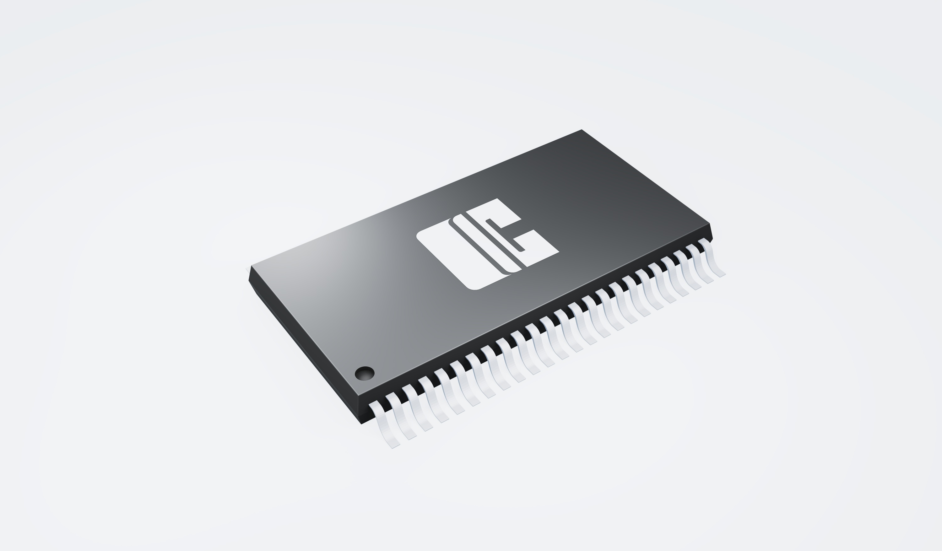
The AiP74LVC/LVCH16373 are 16-bit D-type transparent latches featuring separate D-type inputs with bus hold (AiP74LVCH16373 only) for each latch and 3-state outputs for bus-oriented applications. One Latch Enable (LE) input and one Output Enable( ) are provided for each octal. Inputs can be driven from either 3.3V or 5V devices.When disabled, up to 5.5V can be applied to the outputs. These features allow the use of these devices in mixed 3.3V and 5V applications.The device consists of two sections of eight D-type transparent latches with 3-state true outputs. When LE is HIGH, data at the Dn inputs enter the latches. In this condition, the latches are transparent, that is, the latch outputs change each time its corresponding D-input changes. The latches store the information that was present at the D-inputs one set-up time (tsu) preceding the HIGH-to-LOW transition of LE. When is LOW, the contents of the eight latches are available at the outputs. When is HIGH, the outputs go to the high impedance OFF-state. Operation of the input does not affect the state of the latches. Bus hold on the data inputs eliminates the need for external pull-up resistors to hold unused inputs.
Details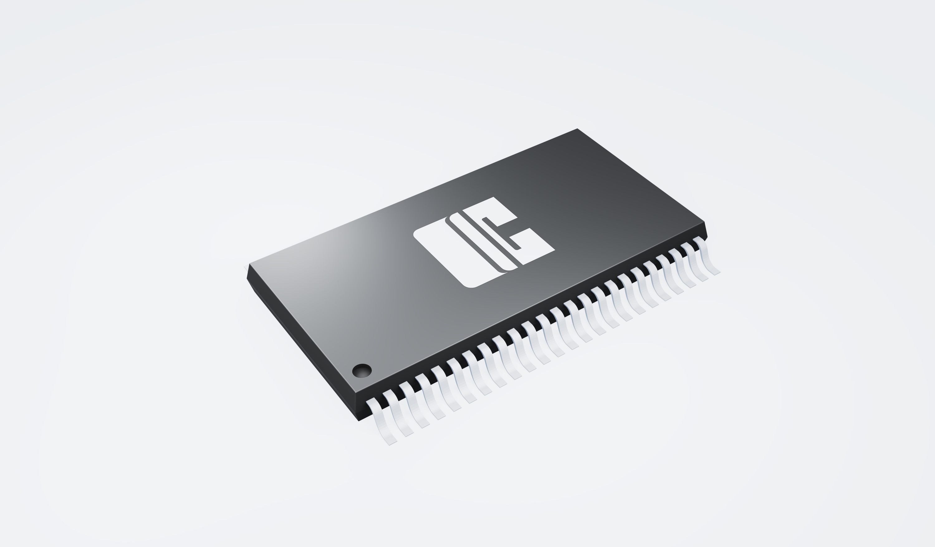
The AiP74LVC/LVCH16373 are 16-bit D-type transparent latches featuring separate D-type inputs with bus hold (AiP74LVCH16373 only) for each latch and 3-state outputs for bus-oriented applications. One Latch Enable (LE) input and one Output Enable( ) are provided for each octal. Inputs can be driven from either 3.3V or 5V devices.When disabled, up to 5.5V can be applied to the outputs. These features allow the use of these devices in mixed 3.3V and 5V applications.The device consists of two sections of eight D-type transparent latches with 3-state true outputs. When LE is HIGH, data at the Dn inputs enter the latches. In this condition, the latches are transparent, that is, the latch outputs change each time its corresponding D-input changes. The latches store the information that was present at the D-inputs one set-up time (tsu) preceding the HIGH-to-LOW transition of LE. When is LOW, the contents of the eight latches are available at the outputs. When is HIGH, the outputs go to the high impedance OFF-state. Operation of the input does not affect the state of the latches. Bus hold on the data inputs eliminates the need for external pull-up resistors to hold unused inputs.
Details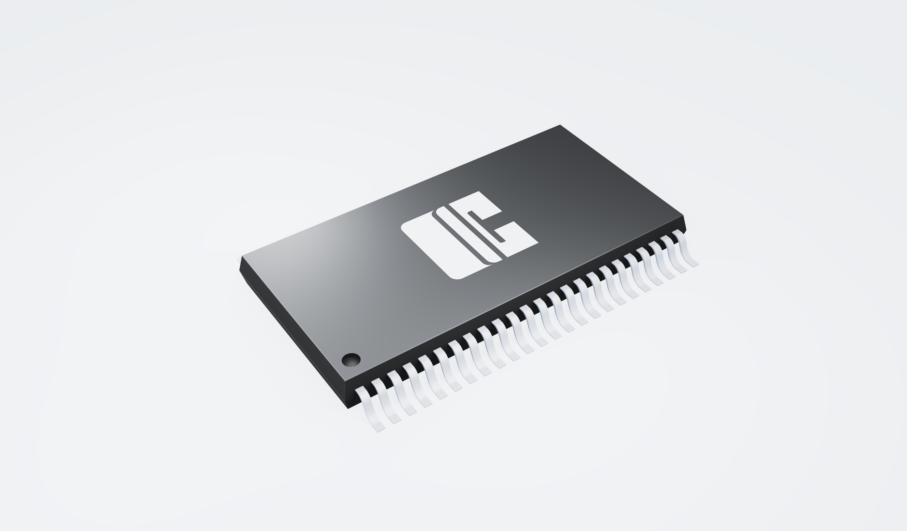
The AiP74LVC/LVCH162373 are 16-bit D-type transparent latches featuring separate D-type inputs with bus hold (AiP74LVCH162373 only) for each latch and 3-state outputs for bus-oriented applications. The input can be driven from either 3.3V or 5V devices. This feature allows the use of this device in a mixed 3.3V and 5V environment.
Details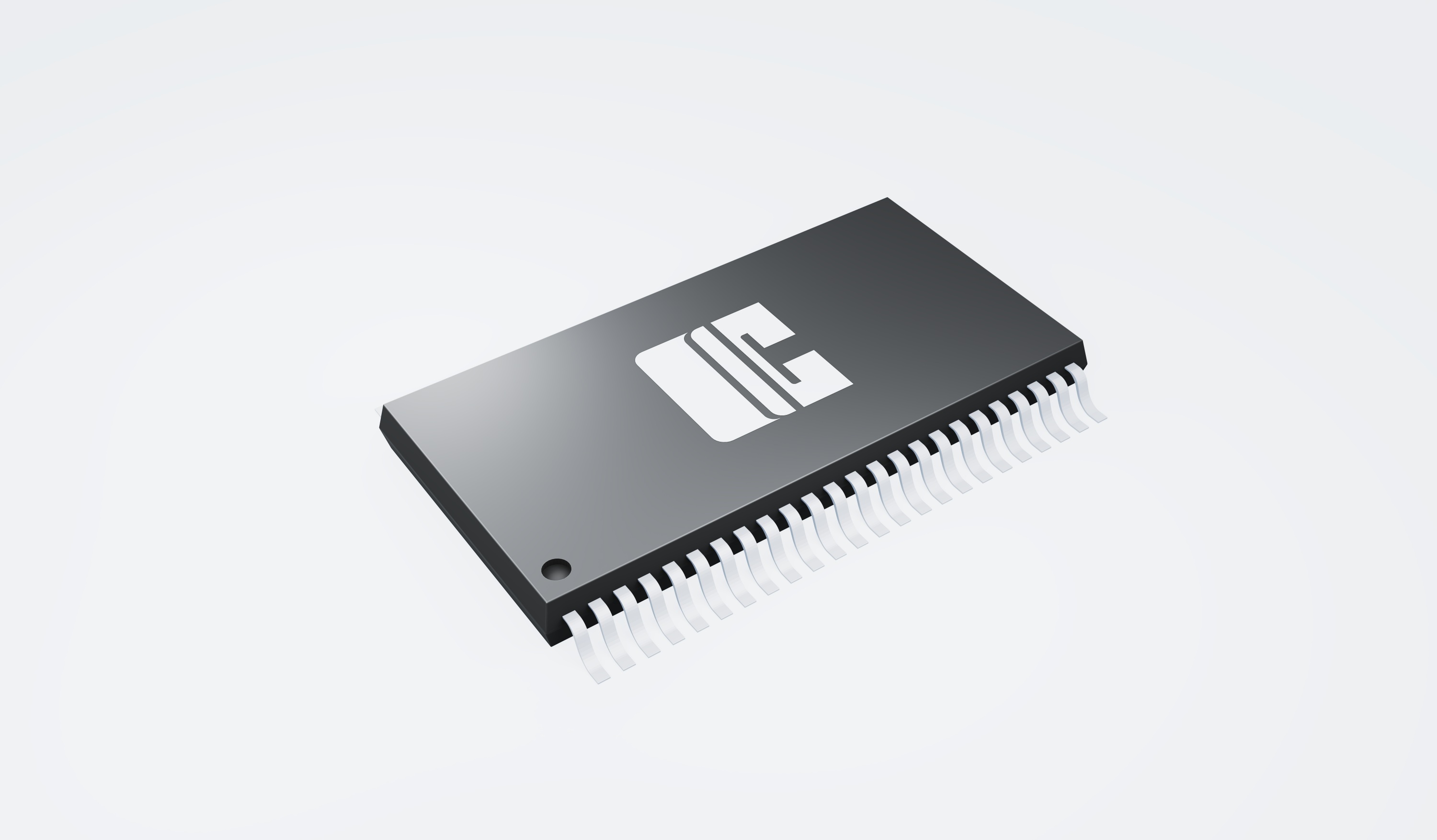
The AiP74LVC/LVCH162373 are 16-bit D-type transparent latches featuring separate D-type inputs with bus hold (AiP74LVCH162373 only) for each latch and 3-state outputs for bus-oriented applications. The input can be driven from either 3.3V or 5V devices. This feature allows the use of this device in a mixed 3.3V and 5V environment.
Details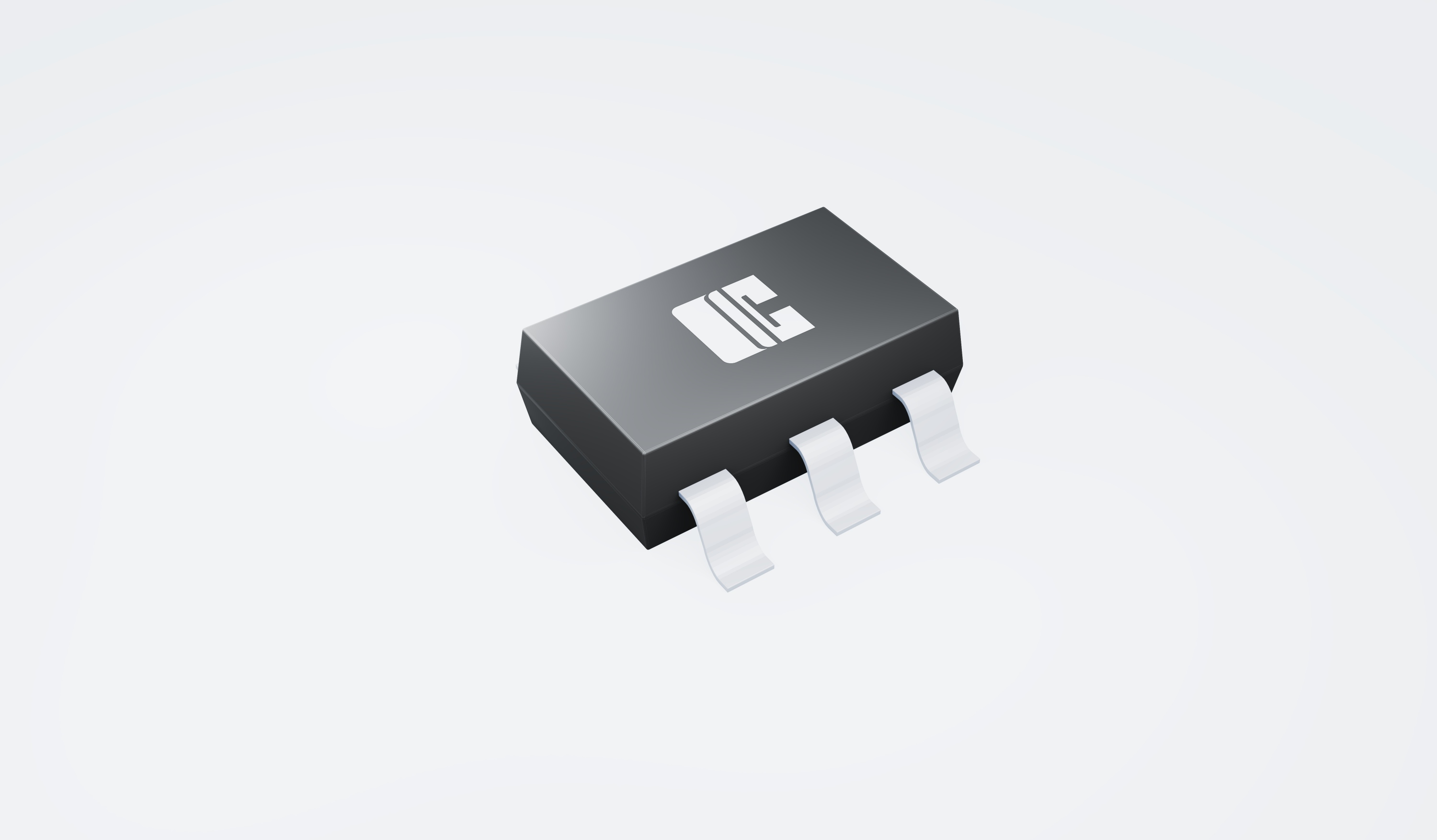
The AiP74LVC1T45; AiP74LVCH1T45 are single bit, dual supply transceivers with 3-state outputs that enable bidirectional level translation. They feature two 1-bit input-output ports (A and B), a direction control input (DIR) and dual supply pins (VCC(A) and VCC(B)). Both VCC(A) and VCC(B) can be supplied at any voltage between 1.2 V and 5.5 V making the device suitable for translating between any of the low voltage nodes (1.2V, 1.5V, 1.8V, 2.5V, 3.3V and 5.0V). Pins A and DIR are referenced to VCC(A) and pin B is referenced to VCC(B). A HIGH on DIR allows transmission from A to B and a LOW on DIR allows transmission from B to A.The devices are fully specified for partial power-down applications using IOFF. The IOFF circuitry disables the output, preventing any damaging backflow current through the device when it is powered down. In suspend mode when either VCC(A) or VCC(B) are at GND level, both A port and B port are in the high-impedance OFF-state.Active bus hold circuitry in the AiP74LVCH1T45 holds unused or floating data inputs at a valid logic level.
Details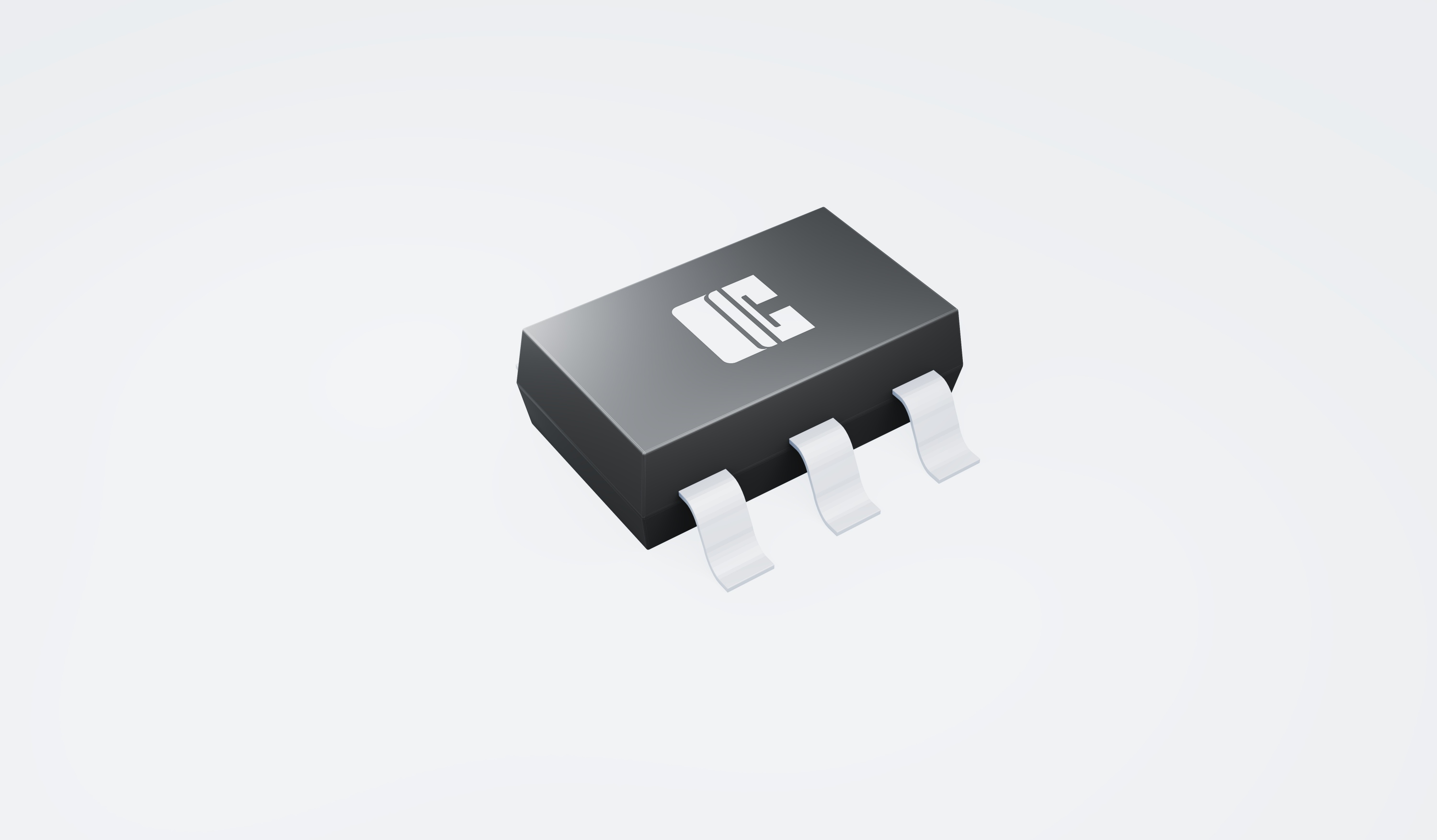
The AiP74LVC1T45; AiP74LVCH1T45 are single bit, dual supply transceivers with 3-state outputs that enable bidirectional level translation. They feature two 1-bit input-output ports (A and B), a direction control input (DIR) and dual supply pins (VCC(A) and VCC(B)). Both VCC(A) and VCC(B) can be supplied at any voltage between 1.2 V and 5.5 V making the device suitable for translating between any of the low voltage nodes (1.2V, 1.5V, 1.8V, 2.5V, 3.3V and 5.0V). Pins A and DIR are referenced to VCC(A) and pin B is referenced to VCC(B). A HIGH on DIR allows transmission from A to B and a LOW on DIR allows transmission from B to A.The devices are fully specified for partial power-down applications using IOFF. The IOFF circuitry disables the output, preventing any damaging backflow current through the device when it is powered down. In suspend mode when either VCC(A) or VCC(B) are at GND level, both A port and B port are in the high-impedance OFF-state.Active bus hold circuitry in the AiP74LVCH1T45 holds unused or floating data inputs at a valid logic level.
Details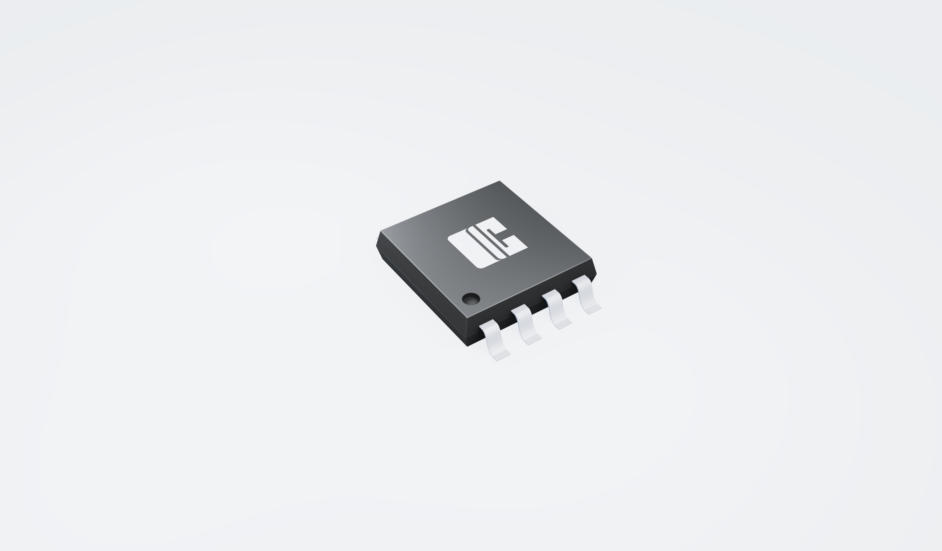
The AiP74LVC2T45; AiP74LVCH2T45 are dual bit, dual supply translating transceivers with 3-state outputs that enable bidirectional level translation. They feature two 2-bits input-output ports(nA and nB), a direction control input (DIR) and dual supply pins (VCC(A) and VCC(B)). Both VCC(A) and VCC(B) can be supplied at any voltage between 1.2V and 5.5V making the device suitable for translating between any of the low voltage nodes (1.2V, 1.5V, 1.8V, 2.5V, 3.3V and 5.0V). Pins nA and DIR are referenced to VCC(A) and pins nB are referenced to VCC(B). A HIGH on DIR allows transmission from nA to nB and a LOW on DIR allows transmission from nB to nA.The devices are fully specified for partial power-down applications using IOFF. The IOFF circuitry disables the output, preventing any damaging backflow current through the device when it is powered down. In suspend mode when either VCC(A) or VCC(B) are at GND level, both A port and B port are in the high-impedance OFF-state.Active bus hold circuitry in the AiP74LVCH2T45 holds unused or floating data inputs at a valid logic level.
Details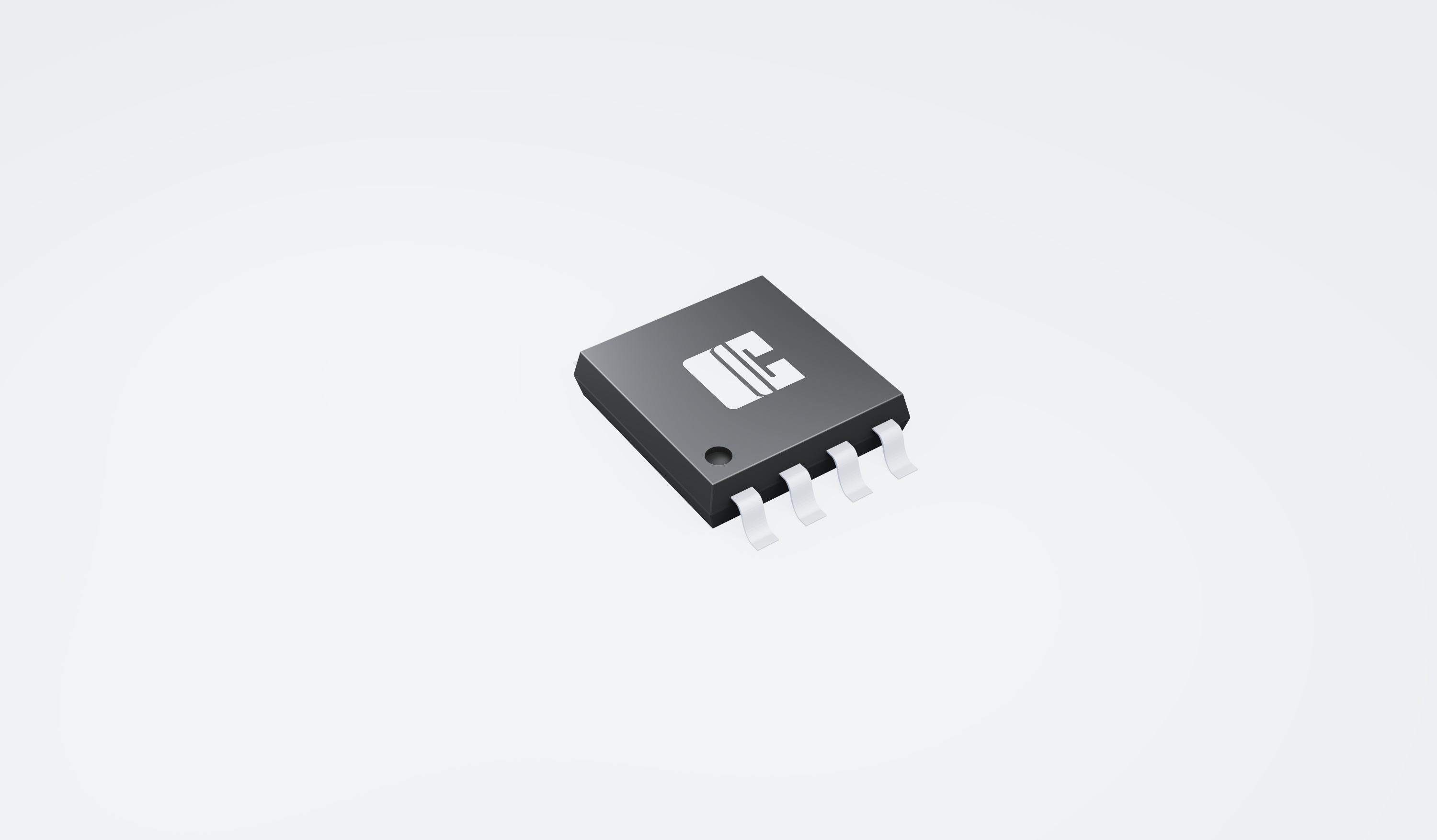
The AiP74LVC2T45; AiP74LVCH2T45 are dual bit, dual supply translating transceivers with 3-state outputs that enable bidirectional level translation. They feature two 2-bits input-output ports(nA and nB), a direction control input (DIR) and dual supply pins (VCC(A) and VCC(B)). Both VCC(A) and VCC(B) can be supplied at any voltage between 1.2V and 5.5V making the device suitable for translating between any of the low voltage nodes (1.2V, 1.5V, 1.8V, 2.5V, 3.3V and 5.0V). Pins nA and DIR are referenced to VCC(A) and pins nB are referenced to VCC(B). A HIGH on DIR allows transmission from nA to nB and a LOW on DIR allows transmission from nB to nA.The devices are fully specified for partial power-down applications using IOFF. The IOFF circuitry disables the output, preventing any damaging backflow current through the device when it is powered down. In suspend mode when either VCC(A) or VCC(B) are at GND level, both A port and B port are in the high-impedance OFF-state.Active bus hold circuitry in the AiP74LVCH2T45 holds unused or floating data inputs at a valid logic level.
Details
The AiP74LVC2T45; AiP74LVCH2T45 are dual bit, dual supply translating transceivers with 3-state outputs that enable bidirectional level translation. They feature two 2-bits input-output ports(nA and nB), a direction control input (DIR) and dual supply pins (VCC(A) and VCC(B)). Both VCC(A) and VCC(B) can be supplied at any voltage between 1.2V and 5.5V making the device suitable for translating between any of the low voltage nodes (1.2V, 1.5V, 1.8V, 2.5V, 3.3V and 5.0V). Pins nA and DIR are referenced to VCC(A) and pins nB are referenced to VCC(B). A HIGH on DIR allows transmission from nA to nB and a LOW on DIR allows transmission from nB to nA.The devices are fully specified for partial power-down applications using IOFF. The IOFF circuitry disables the output, preventing any damaging backflow current through the device when it is powered down. In suspend mode when either VCC(A) or VCC(B) are at GND level, both A port and B port are in the high-impedance OFF-state.Active bus hold circuitry in the AiP74LVCH2T45 holds unused or floating data inputs at a valid logic level.
Details
The AiP74LVC/LVCH4T245 are 4-bit dual supply translating transceivers with 3-state outputs that enable bidirectional level translation. The device can be used as two 2-bit transceivers or as a 4-bit transceiver . It features four 2-bit input-output ports (nAn and nBn), a direction control input (nDIR), a output enable input (n ) and dual supply pins (VCC(A) and VCC(B)).Both VCC(A) and VCC(B) can be supplied at any voltage between 1.2V and 5.5V making the device suitable for translating between any of the low voltage nodes (1.2V, 1.5V, 1.8V, 2.5V, 3.3V and 5.0V). Pins nAn, n and nDIR are referenced to VCC(A) and pins nBn are referenced to VCC(B). A HIGH on nDIR allows transmission from nAn to nBn and a LOW on nDIR allows transmission from nBn to nAn. The output enable input (n ) can be used to disable the outputs so the buses are effectively isolated.The devices are fully specified for partial power-down applications using IOFF. The IOFF circuitry disables the output, preventing any damaging backflow current through the device when it is powered down. In suspend mode when either VCC(A) or VCC(B) are at GND level, both nAn port and nBn port are in the high-impedance OFF-state. Active bus hold circuitry in the AiP74LVCH4T245 holds unused or floating data inputs at a valid logic level.
Details
The AiP74LVC/LVCH4T774 is a 4-bit, dual supply transceiver that enables bidirectional level translation. It features eight 1-bit input-output ports (An and Bn), four direction control inputs (DIR1, DIR2, DIR3 and DIR4), an output enable input ( ) and dual supply pins (VCC(A) and VCC(B)). Both VCC(A) and VCC(B) can be supplied at any voltage between 1.2V and 5.5V making the device suitable for translating between any of the low voltage nodes (1.2V, 1.5V, 1.8V, 2.5V, 3.3V, 5V). Pins An, and DIRn are referenced to VCC(A) and pins Bn are referenced to VCC(B). A HIGH on DIRn allows transmission from An to Bn and a LOW on DIRn allows transmission from Bn to An. The output enable input ( ) can be used to disable the outputs so the buses are effectively isolated.The device is fully specified for partial power-down applications using IOFF. The IOFF circuitry disables the output, preventing any damaging backflow current through the device when it is powered down. In suspend mode when either VCC(A) or VCC(B) are at GND level, both An and Bn are in the high-impedance OFF-state.Active bus hold circuitry in the AiP74LVCH4T774 holds unused or floating data inputs at a valid logic level.
Details
The AiP74LVC/LVCH4T774 is a 4-bit, dual supply transceiver that enables bidirectional level translation. It features eight 1-bit input-output ports (An and Bn), four direction control inputs (DIR1, DIR2, DIR3 and DIR4), an output enable input ( ) and dual supply pins (VCC(A) and VCC(B)). Both VCC(A) and VCC(B) can be supplied at any voltage between 1.2V and 5.5V making the device suitable for translating between any of the low voltage nodes (1.2V, 1.5V, 1.8V, 2.5V, 3.3V, 5V). Pins An, and DIRn are referenced to VCC(A) and pins Bn are referenced to VCC(B). A HIGH on DIRn allows transmission from An to Bn and a LOW on DIRn allows transmission from Bn to An. The output enable input ( ) can be used to disable the outputs so the buses are effectively isolated.The device is fully specified for partial power-down applications using IOFF. The IOFF circuitry disables the output, preventing any damaging backflow current through the device when it is powered down. In suspend mode when either VCC(A) or VCC(B) are at GND level, both An and Bn are in the high-impedance OFF-state.Active bus hold circuitry in the AiP74LVCH4T774 holds unused or floating data inputs at a valid logic level.
Details
The AiP74LVC/LVCH8T245 are 8-bit dual supply translating transceivers with 3-state outputs that enable bidirectional level translation. They feature two data input-output ports (pins An and Bn), a direction control input (DIR), an output enable input ( ) and dual supply pins (VCC(A) and VCC(B)). Both VCC(A) and VCC(B) can be supplied at any voltage between 1.2V and 5.5V making the device suitable for translating between any of the low voltage nodes (1.2V, 1.5V, 1.8V, 2.5V, 3.3V and 5.0V). Pins An, and DIR are referenced to VCC(A) and pins Bn are referenced to VCC(B). A HIGH on DIR allows transmission from An to Bn and a LOW on DIR allows transmission from Bn to An. The output enable input ( ) can be used to disable the outputs so the buses are effectively isolated.The devices are fully specified for partial power-down applications using IOFF. The IOFF circuitry disables the output, preventing any damaging backflow current through the device when it is powered down. In suspend mode when either VCC(A) or VCC(B) are at GND level, both A port and B port are in the high-impedance OFF-state. Active bus hold circuitry in the AiP74LVCH8T245 holds unused or floating data inputs at a valid logic level.
Details
The AiP74LVC/LVCH8T245 are 8-bit dual supply translating transceivers with 3-state outputs that enable bidirectional level translation. They feature two data input-output ports (pins An and Bn), a direction control input (DIR), an output enable input ( ) and dual supply pins (VCC(A) and VCC(B)). Both VCC(A) and VCC(B) can be supplied at any voltage between 1.2V and 5.5V making the device suitable for translating between any of the low voltage nodes (1.2V, 1.5V, 1.8V, 2.5V, 3.3V and 5.0V). Pins An, and DIR are referenced to VCC(A) and pins Bn are referenced to VCC(B). A HIGH on DIR allows transmission from An to Bn and a LOW on DIR allows transmission from Bn to An. The output enable input ( ) can be used to disable the outputs so the buses are effectively isolated.The devices are fully specified for partial power-down applications using IOFF. The IOFF circuitry disables the output, preventing any damaging backflow current through the device when it is powered down. In suspend mode when either VCC(A) or VCC(B) are at GND level, both A port and B port are in the high-impedance OFF-state. Active bus hold circuitry in the AiP74LVCH8T245 holds unused or floating data inputs at a valid logic level.
Details
The AiP74LVC/LVCH16T245 are 16-bit dual supply translating transceivers with 3-state outputs that enable bidirectional level translation.The device can be used as two 8-bit transceivers or as a 16-bit transceiver.It has dual supplies (VCC(A) and VCC(B)) for voltage translation and four 8-bit input-output ports (nAn and nBn) each with its own output enable (n ) and send/receive (nDIR) input for direction control.Both VCC(A) and VCC(B) can be supplied at any voltage between 1.2V and 5.5V making the device suitable for translating between any of the low voltage nodes (1.2V, 1.5V, 1.8V, 2.5V, 3.3V and 5.0V). Pins nAn, n and nDIR are referenced to VCC(A) and pins nBn are referenced to VCC(B). A HIGH on nDIR allows transmission from nAn to nBn and a LOW on nDIR allows transmission from nBn to nAn. The output enable input (n ) can be used to disable the outputs so the buses are effectively isolated.The devices are fully specified for partial power-down applications using IOFF. The IOFF circuitry disables the output, preventing any damaging backflow current through the device when it is powered down. In suspend mode when either VCC(A) or VCC(B) are at GND level, both nAn port and nBn port are in the high-impedance OFF-state. Active bus hold circuitry in the AiP74LVCH16T245 holds unused or floating data inputs at a valid logic level.
Details
The AiP74LVC/LVCH16T245 are 16-bit dual supply translating transceivers with 3-state outputs that enable bidirectional level translation.The device can be used as two 8-bit transceivers or as a 16-bit transceiver.It has dual supplies (VCC(A) and VCC(B)) for voltage translation and four 8-bit input-output ports (nAn and nBn) each with its own output enable (n ) and send/receive (nDIR) input for direction control.Both VCC(A) and VCC(B) can be supplied at any voltage between 1.2V and 5.5V making the device suitable for translating between any of the low voltage nodes (1.2V, 1.5V, 1.8V, 2.5V, 3.3V and 5.0V). Pins nAn, n and nDIR are referenced to VCC(A) and pins nBn are referenced to VCC(B). A HIGH on nDIR allows transmission from nAn to nBn and a LOW on nDIR allows transmission from nBn to nAn. The output enable input (n ) can be used to disable the outputs so the buses are effectively isolated.The devices are fully specified for partial power-down applications using IOFF. The IOFF circuitry disables the output, preventing any damaging backflow current through the device when it is powered down. In suspend mode when either VCC(A) or VCC(B) are at GND level, both nAn port and nBn port are in the high-impedance OFF-state. Active bus hold circuitry in the AiP74LVCH16T245 holds unused or floating data inputs at a valid logic level.
Details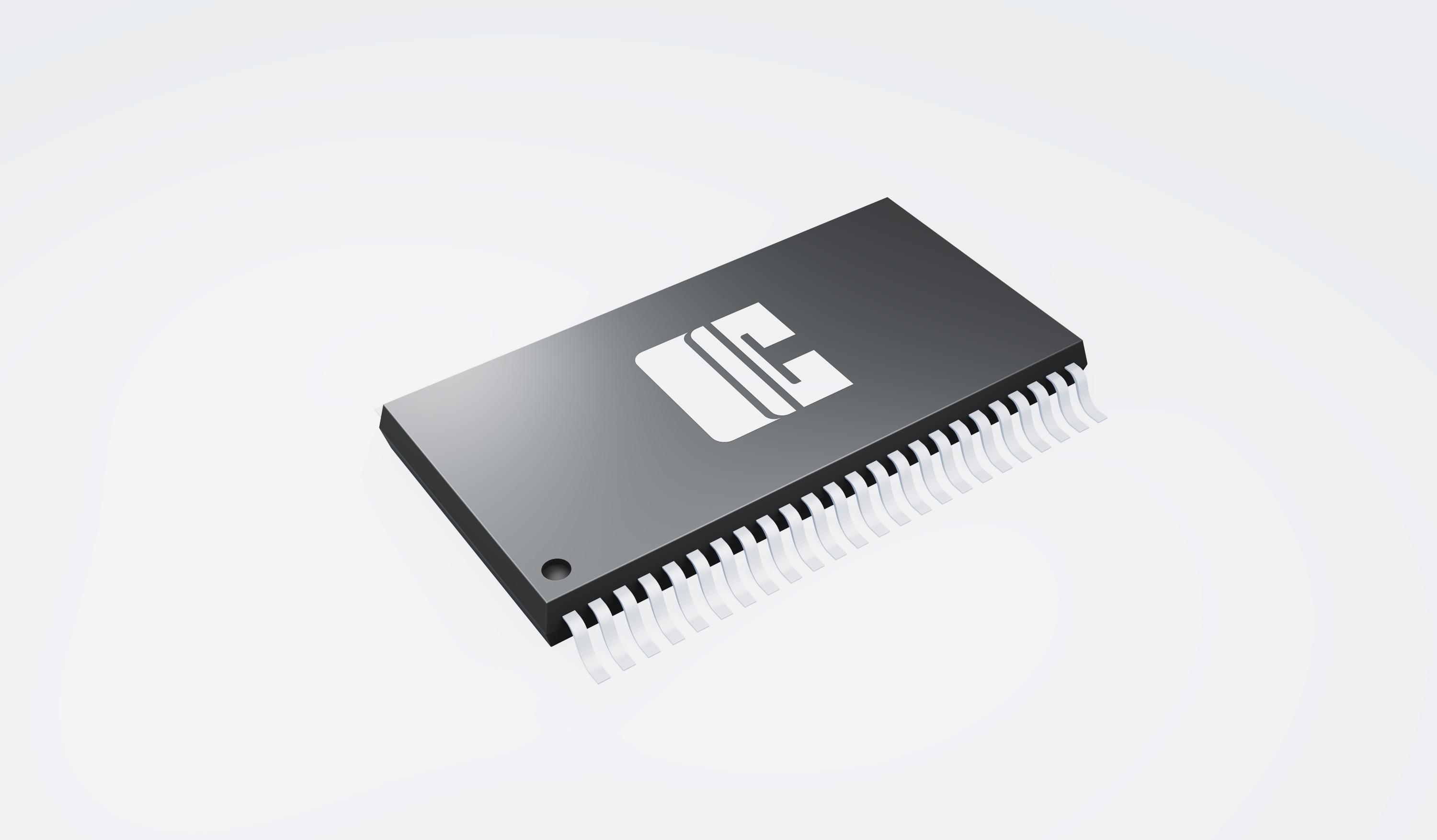
The AiP74ALVC164245 is a high-performance, low-power, low-voltage, Si-gate CMOS device,superior to most advanced CMOS compatible TTL families.The AiP74ALVC164245 is a 16-bit (dual octal) dual supply translating transceiver featuring non-inverting 3-state bus compatible outputs in both send and receive directions. It is designed to interface between a 3V and 5V bus in a mixed 3V and 5V supply environment.This device can be used as two 8-bit transceivers or one 16-bit transceiver.The direction control inputs (1DIR and 2DIR) determine the direction of the data flow.nDIR (active HIGH) enables data from nAn ports to nBn ports. nDIR (active LOW) enables data from nBn ports to nAn ports. The output enable inputs (1 and 2 ), when HIGH, disable both nAn and nBn ports by placing them in a high-impedance OFF-state. Pins nAn, n and nDIR are referenced to VCC(A) and pins nBn are referenced to VCC(B).In suspend mode, when one of the supply voltages is zero, there will be no current flow from the non-zero supply towards the zero supply. The nAn-outputs must be set 3-state and the voltage on the A-bus must be smaller than Vdiode (typical 0.7V). VCC(B)≥VCC(A) (except in suspend mode).
Details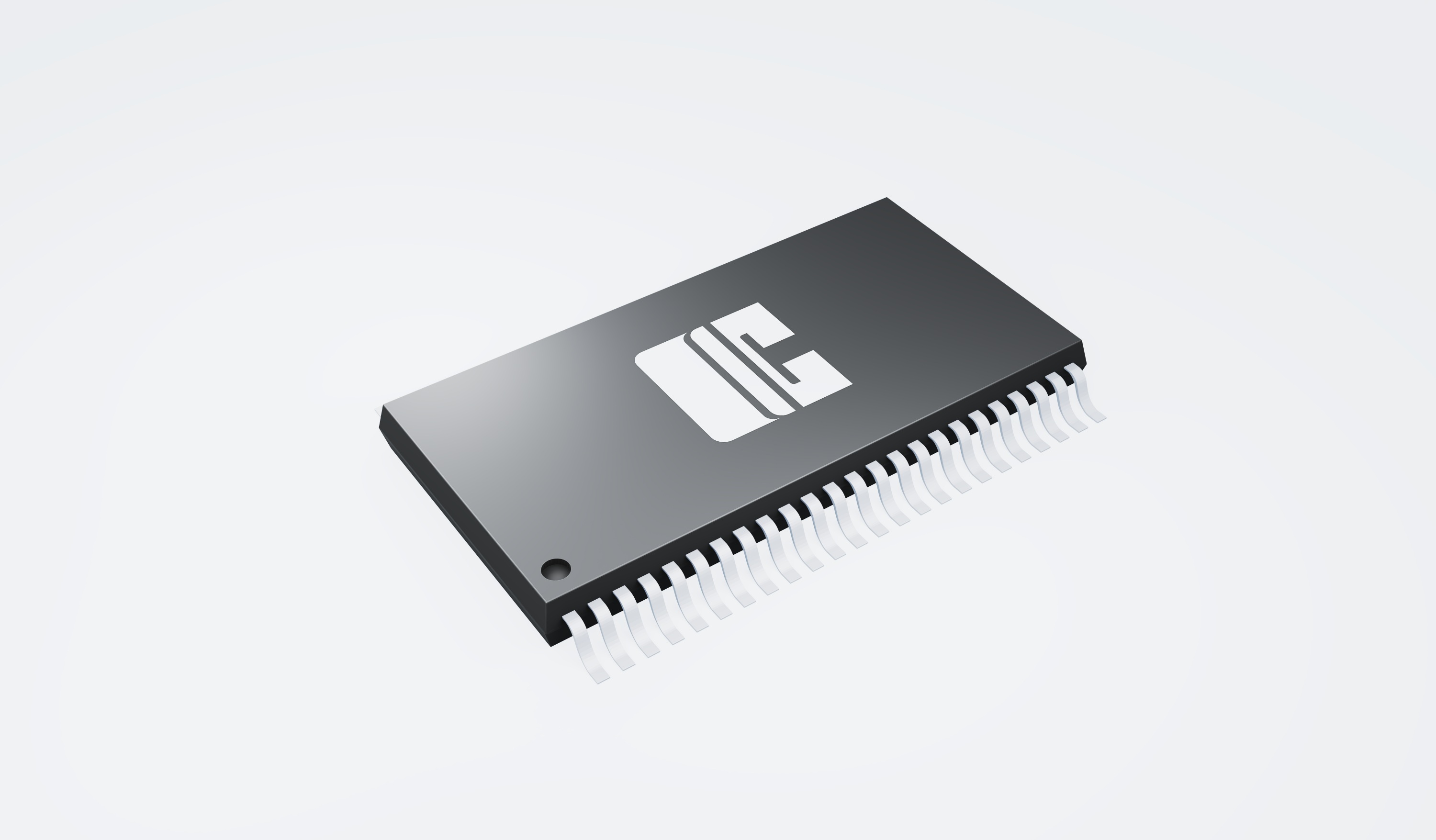
The AiP74ALVC/ALVCH162374 are 16-bit Edge-triggered D-type Flip-flop with 3-state outputs.The input can be driven from either 3.3V or 5V devices. This feature allows the use of this device in a mixed 3.3V and 5V environment.
Details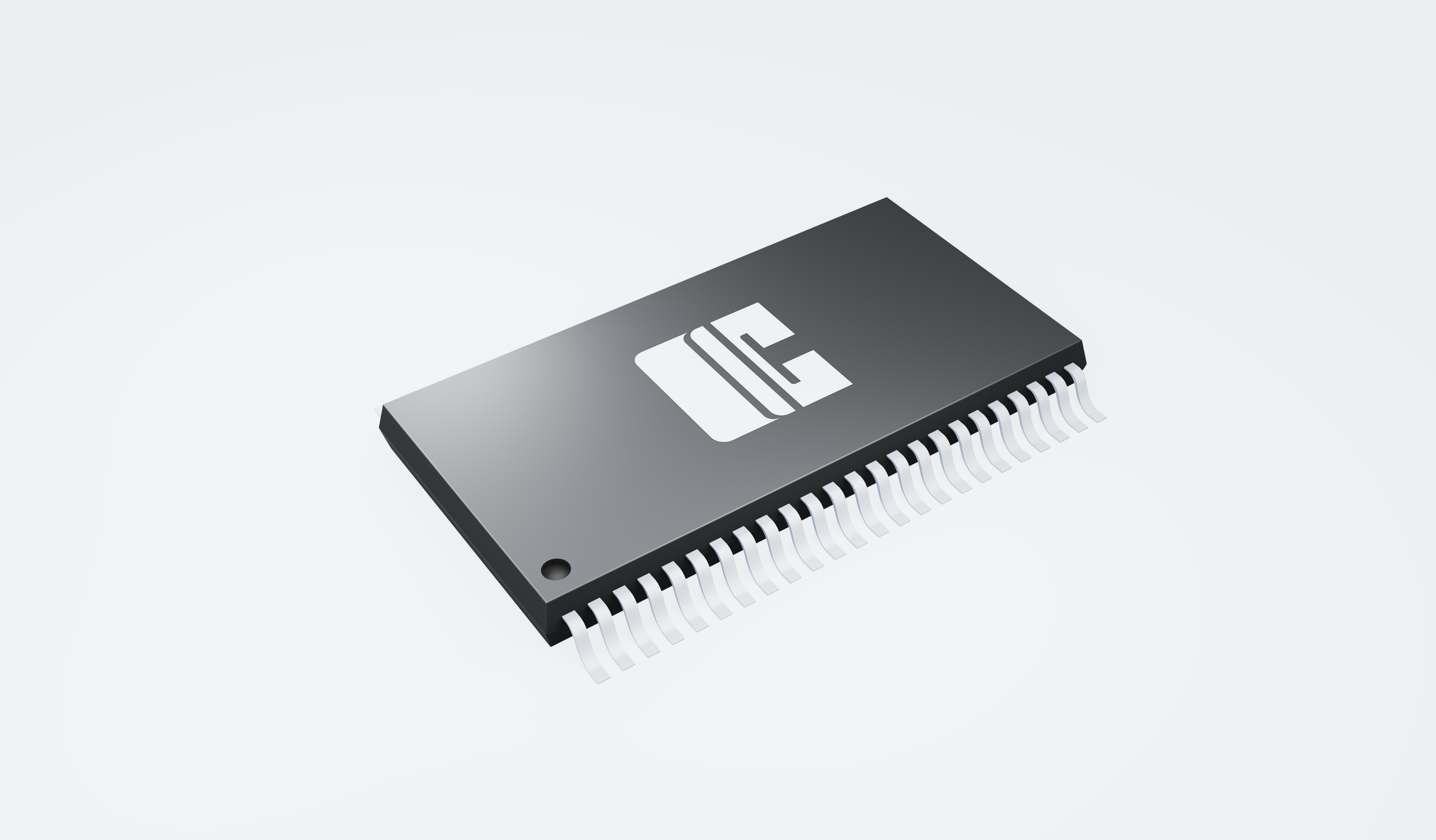
The AiP74ALVC/ALVCH162374 are 16-bit Edge-triggered D-type Flip-flop with 3-state outputs.The input can be driven from either 3.3V or 5V devices. This feature allows the use of this device in a mixed 3.3V and 5V environment.
Details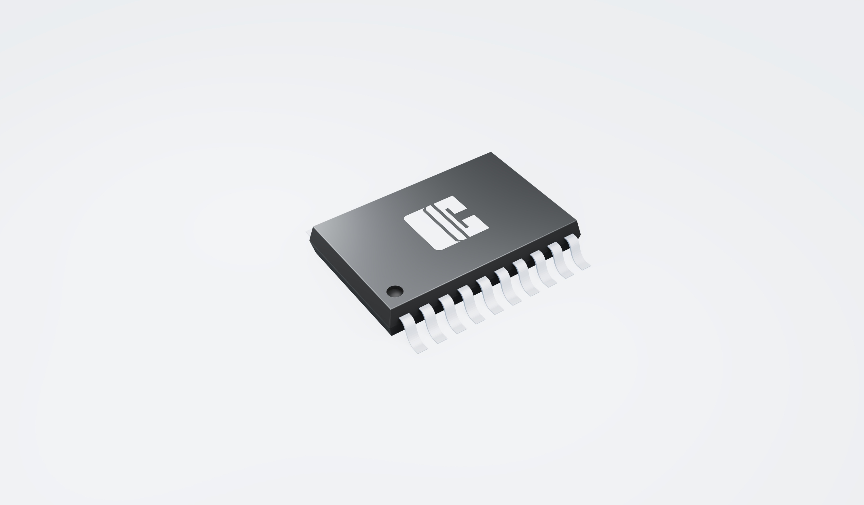
The AiP74LVT244/LVTH244 is an octal buffer that is ideal for driving bus lines. The device features two output enables (1 , 2 ), each controlling four of the 3-state outputs.
Details
The AiP74LVT244/LVTH244 is an octal buffer that is ideal for driving bus lines. The device features two output enables (1 , 2 ), each controlling four of the 3-state outputs.
Details
The AiP74LVT245; AiP74LVTH245 is an octal transceiver featuring non-inverting 3-state bus compatible outputs in both send and receive directions. The control function implementation minimizes external timing requirements. It features an output enable ( ) input for easy cascading and a direction (DIR) input for direction control.
Details
This device is an octal buffer that is ideal for driving bus lines. The device features two output enables (1 , 2 ), each controlling four of the 3-state outputs.The AiP74LVT2244 is designed with series resistance in both the HIGH and LOW states of the output. This design reduces line noise in applications such as memory address drivers, clock drivers, and bus receivers/transmitters.
Details
This device is an octal transceiver featuring non-inverting 3-state bus compatible outputs in both send and receive directions. The control function implementation minimizes external timing requirements. The device features an output enable input ( ) for easy cascading and a direction input (DIR) for direction control.The AiP74LVT/LVTH2245 is designed with series resistance in both the HIGH state and LOW-state of the output. This design reduces line noise in applications such as memory address drivers, clock drivers and bus transceivers and transmitters.
Details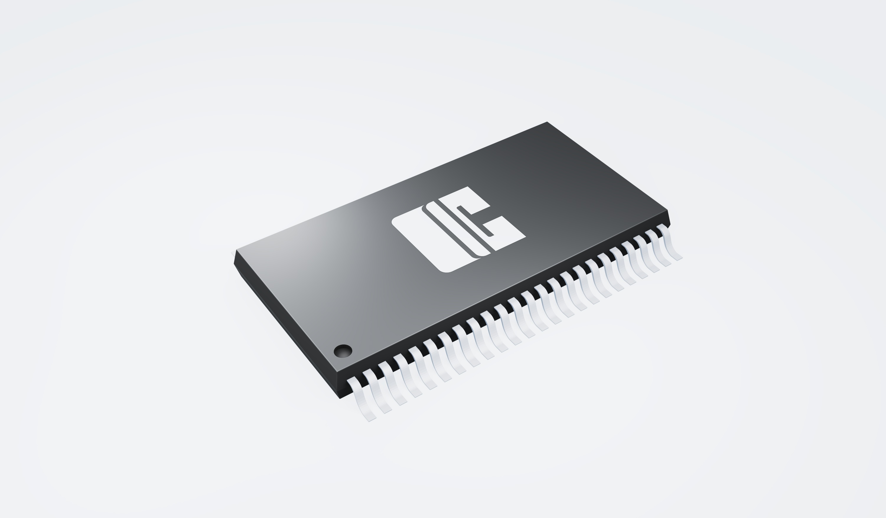
The AiP74LVT16240; AiP74LVTH16240 is an inverting 16-bit buffer that is ideal for driving bus lines.
Details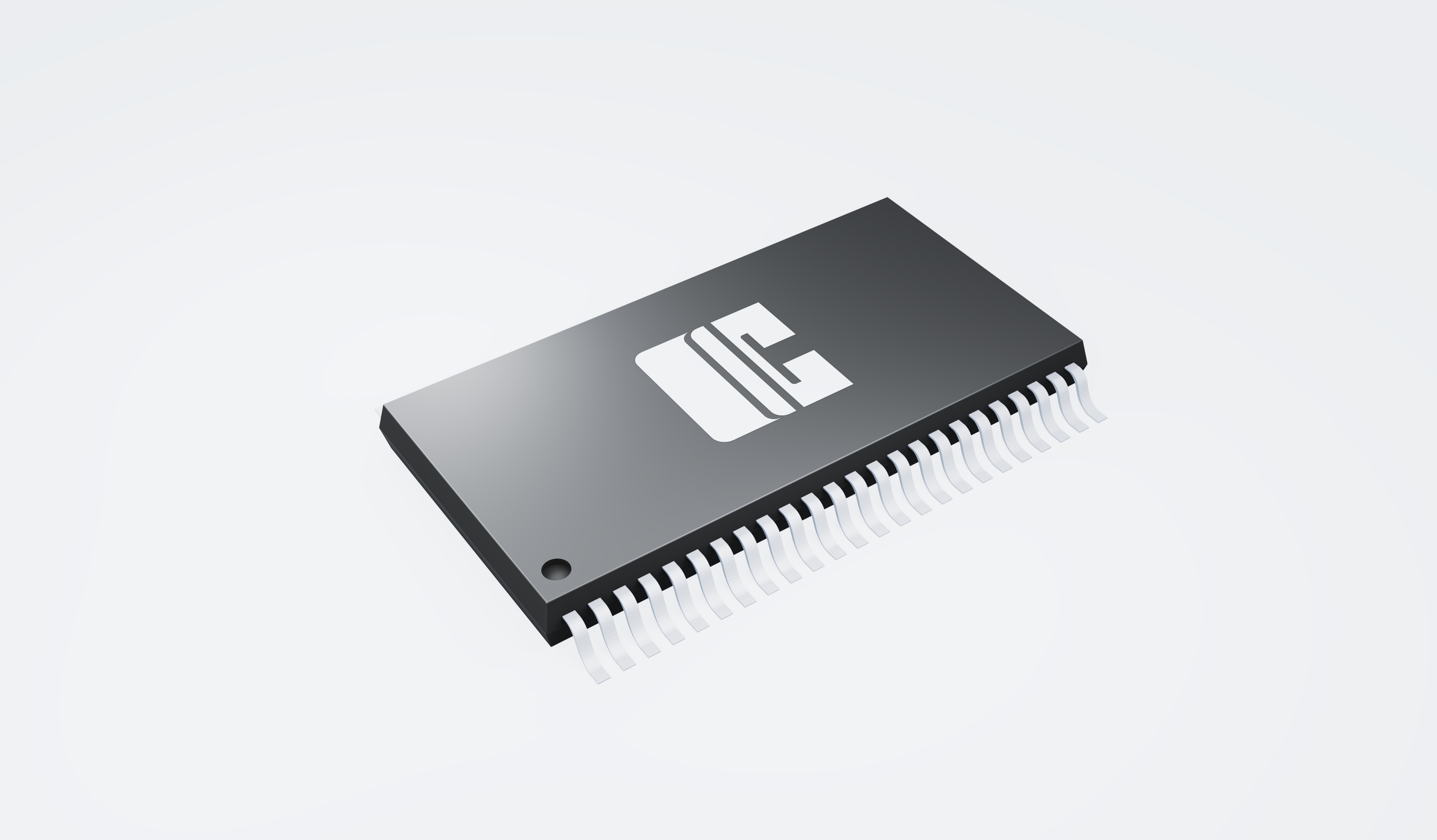
The AiP74LVT16244; AiP74LVTH16244 is a 16-bit buffer and line driver featuring non-inverting 3-state bus outputs. The device can be used as four 4-bit buffers, two 8-bit buffers, or one 16-bit buffer.
Details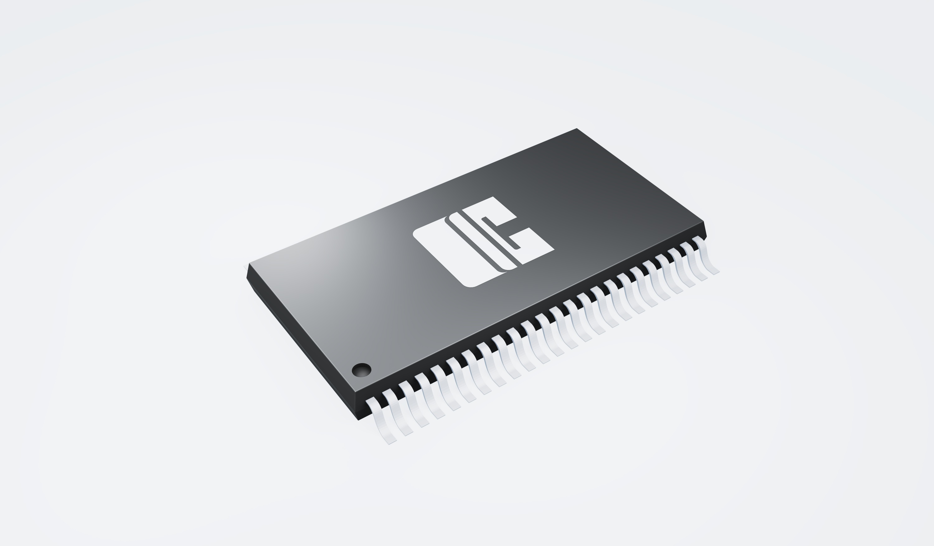
The AiP74LVT16244; AiP74LVTH16244 is a 16-bit buffer and line driver featuring non-inverting 3-state bus outputs. The device can be used as four 4-bit buffers, two 8-bit buffers, or one 16-bit buffer.
Details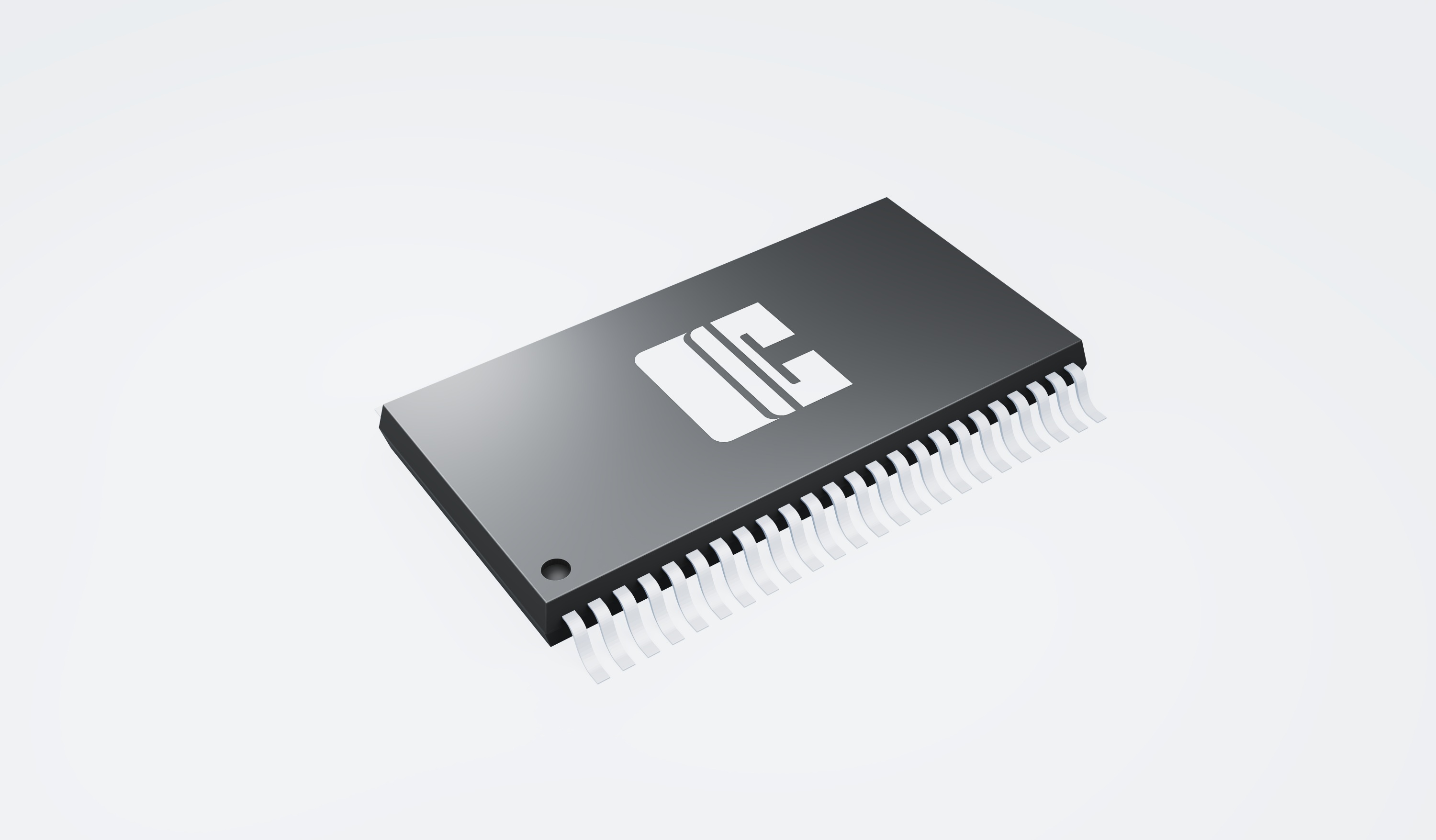
The AiP74LVT16245; AiP74LVTH16245 is a high-performance BiCMOS product designed for VCC operation at 3.3V.This device is a 16-bit transceiver featuring non-inverting 3-state bus compatible outputs in both send and receive directions. The control function implementation minimizes external timing requirements. The device features an output enable input (n ) for easy cascading and a direction input (nDIR) for direction control.
Details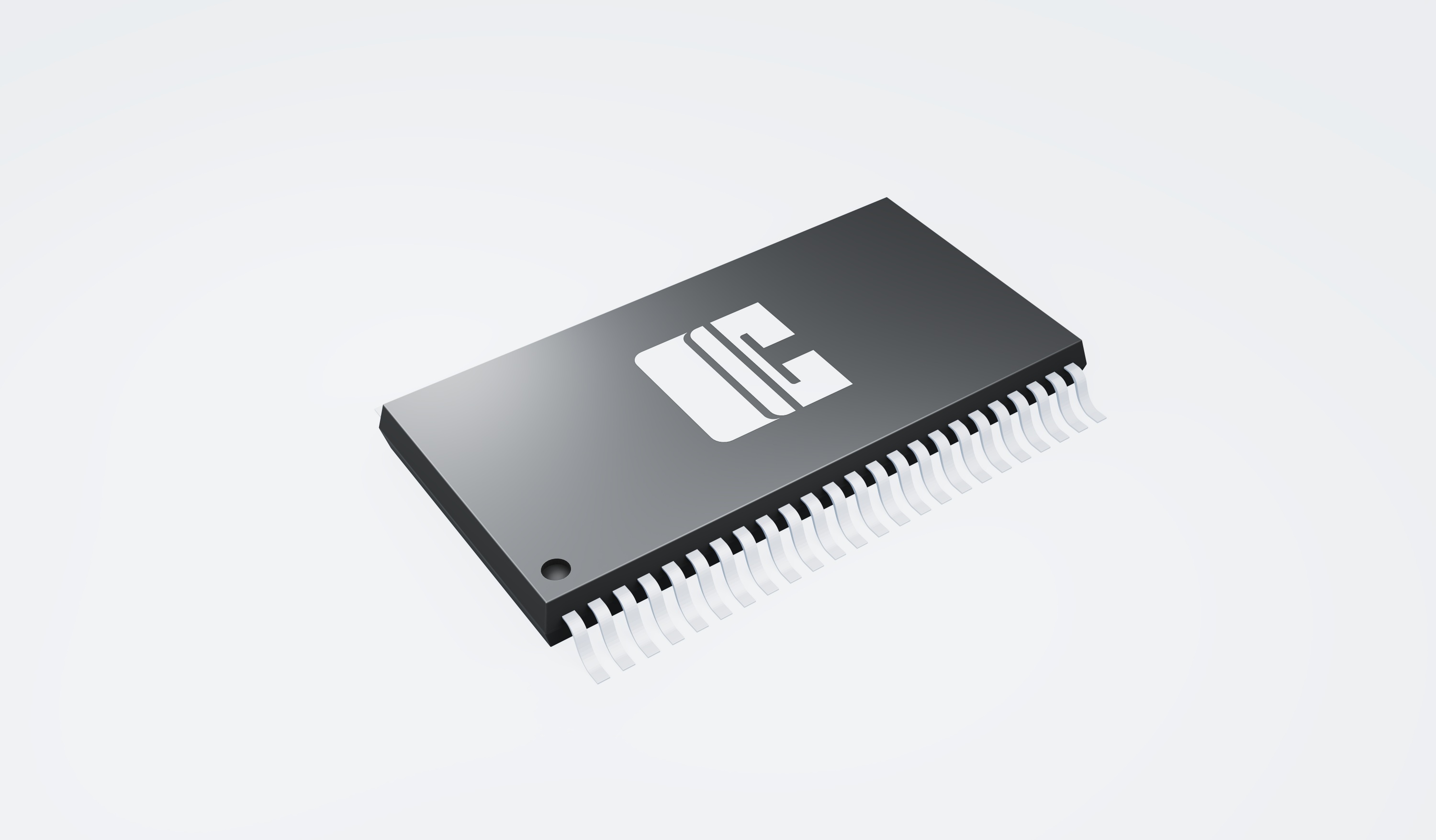
The AiP74LVT16245; AiP74LVTH16245 is a high-performance BiCMOS product designed for VCC operation at 3.3V.This device is a 16-bit transceiver featuring non-inverting 3-state bus compatible outputs in both send and receive directions. The control function implementation minimizes external timing requirements. The device features an output enable input (n ) for easy cascading and a direction input (nDIR) for direction control.
Details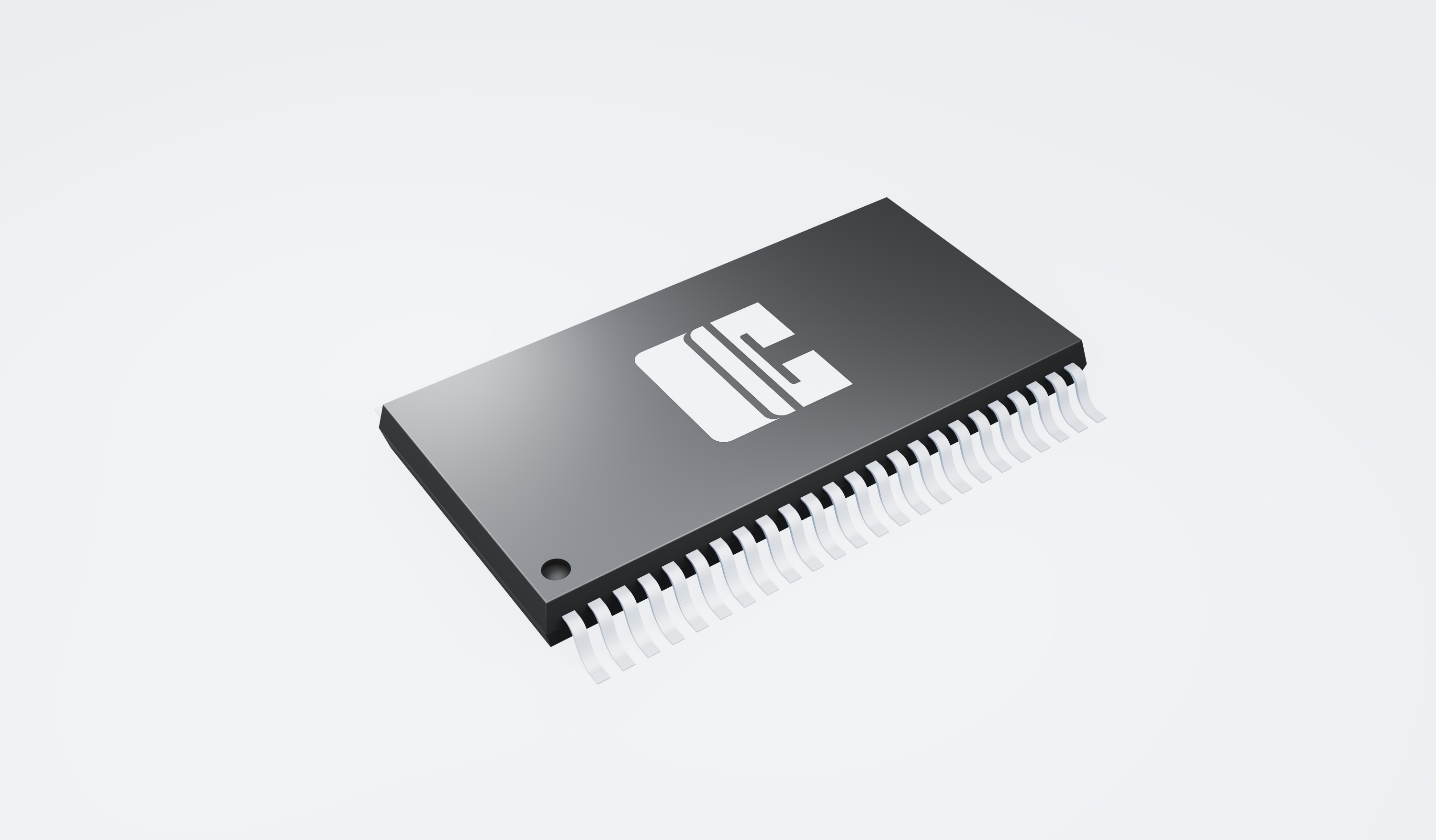
The AiP74LVT16373 is a high-performance BiCMOS product designed for VCC operation at 3.3V.This device is a 16-bit transparent D-type latch with non-inverting 3-state bus compatible outputs.The device can be used as two 8-bit latches or one 16-bit latch. When latch enable (LE) input is HIGH, the Q outputs follow the data (D) inputs. When latch enable is taken LOW, the Q outputs are latched at the levels of the D inputs one setup time prior to the HIGH-to-LOW transition.
Details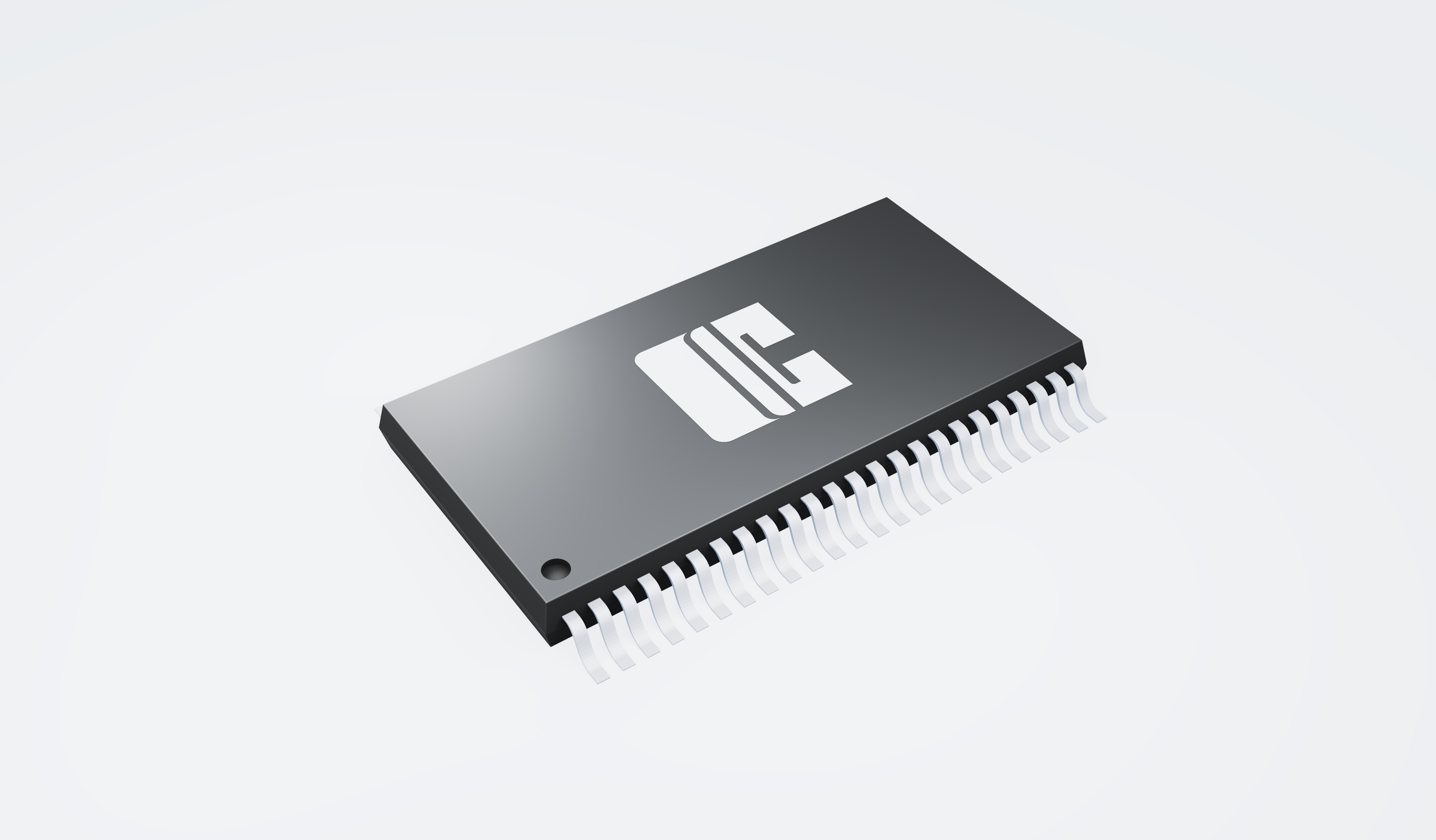
The AiP74LVT16374; AiP74LVTH16374 are high performance BiCMOS products designed for VCC operation at 3.3V.This device is a 16-bit edge-triggered D-type flip-flop featuring non-inverting 3-state outputs. The device can be used as two 8-bit flip-flops or one 16-bit flip-flop. On the positive transition of the clock (nCP), the nQn outputs of the flip-flop take on the logic levels set up at the nDn inputs.
Details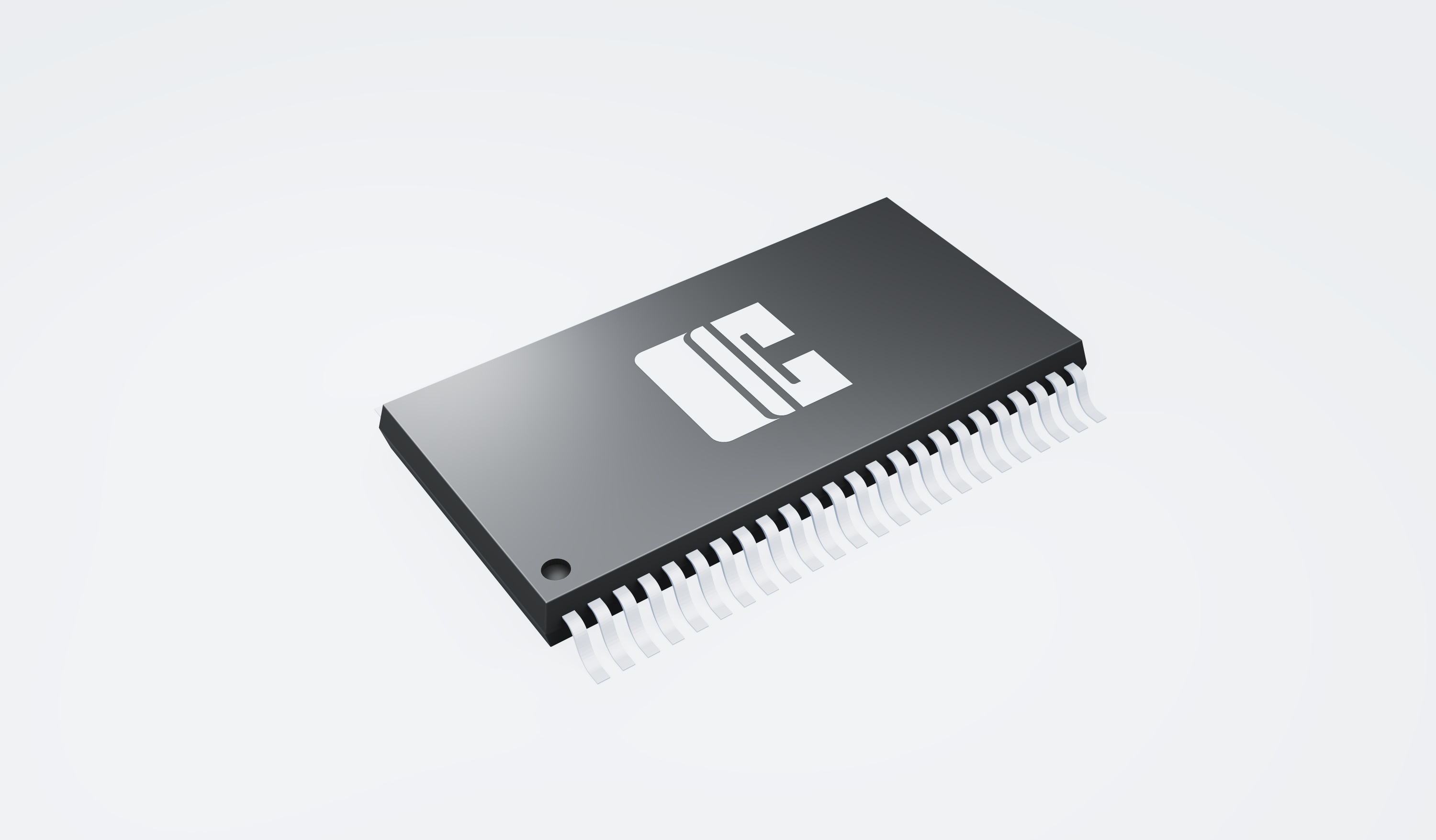
The AiP74LVT16374; AiP74LVTH16374 are high performance BiCMOS products designed for VCC operation at 3.3V.This device is a 16-bit edge-triggered D-type flip-flop featuring non-inverting 3-state outputs. The device can be used as two 8-bit flip-flops or one 16-bit flip-flop. On the positive transition of the clock (nCP), the nQn outputs of the flip-flop take on the logic levels set up at the nDn inputs.
Details
The AiP74AC74 is a dual edge triggered D-type flip-flop with individual data (nD) inputs, clock(nCP) inputs, set (nS—D) and (nR—D) inputs, and complementary nQ and nQ—outputs. The set and rest are asynchronous active LOW inputs and operate independently of the clock input. Information on the data input is transferred to the nQ output on the LOW-to-HIGH transition of the clock pulse. The nD inputs must be stable one set-up time prior to the LOW-to-HIGH clock transition, for predictable operation.
Details
The AiP74ACT74 is a dual edge triggered D-type flip-flop with individual data (nD) inputs, clock (nCP) inputs, set (nS—D) and (nR—D) inputs, and complementary nQ and nQ—outputs. The set and rest are asynchronous active LOW inputs and operate independently of the clock input. Information on the data input is transferred to the nQ output on the LOW-to-HIGH transition of the clock pulse. The nD inputs must be stable one set-up time prior to the LOW-to-HIGH clock transition, for predictable operation.
Details
The AiP74AVC2T45 is a dual-bit, dual-supply transceiver that enables bidirectional level translation. It features two data input-output ports (nA and nB), a direction control input (DIR) and dual-supply pins (VCC(A) and VCC(B)). Both VCC(A) and VCC(B) can be supplied at any voltage between 0.8V and 3.6V making the device suitable for translating between any of the low voltage nodes (0.8V, 1.2V, 1.5V, 1.8V, 2.5V and 3.3V). Pins nA and DIR are referenced to VCC(A) and pins nB are referenced to VCC(B). A HIGH on DIR allows transmission from nA to nB and a LOW on DIR allows transmission from nB to nA.The device is fully specified for partial power-down applications using IOFF. The IOFF circuitry disables the output, preventing any damaging backflow current through the device when it is powered down. In Suspend mode when either VCC(A) or VCC(B) are at GND level, both A and B are in the high-impedance OFF-state.
Details
The AiP74AVCH2T45 is a dual bit, dual supply transceiver that enables bidirectional level translation. It features two data input-output ports (nA and nB), a direction control input(DIR) and dual supply pins (VCC(A) and VCC(B)). Both VCC(A) and VCC(B) can be supplied at any voltage between 0.8V and 3.6V making the device suitable for translating between any of the low voltage nodes (0.8V, 1.2V, 1.5V, 1.8V, 2.5V and 3.3V). Pins nA and DIR are referenced to VCC(A) and pins nB are referenced to VCC(B). A HIGH on DIR allows transmission from nA to nB and a LOW on DIR allows transmission from nB to nA.The device is fully specified for partial power-down applications using IOFF. The IOFF circuitry disables the output, preventing any damaging backflow current through the device when it is powered down. In suspend mode when either VCC(A) or VCC(B) are at GND level, both A and B are in the high-impedance OFF-state.The AiP74AVCH2T45 has active bus hold circuitry which is provided to hold unused or floating data inputs at a valid logic level. This feature eliminates the need for external pull-up or pull-down resistors.
Details
The AiP74AVC4T245 is an 4-bit, dual supply transceiver that enables bidirectional level translation. The device can be used as two 2-bit transceivers or as a 4-bit transceiver. It features four 2-bit input-output ports (nAn and nBn), a direction control input (nDIR), a output enable input (n ) and dual supply pins (VCC(A) and VCC(B)). Both VCC(A) and VCC(B) can be supplied at any voltage between 0.8V and 3.6V making the device suitable for translating between any of the low voltage nodes (0.8V, 1.2V, 1.5V, 1.8V, 2.5V and 3.3V). Pins nAn, n and nDIR are referenced to VCC(A) and pins nBn are referenced to VCC(B). A HIGH on nDIR allows transmission from nAn to nBn and a LOW on nDIR allows transmission from nBn to nAn. The output enable input (n ) can be used to disable the outputs so the buses are effectively isolated.The device is fully specified for partial power-down applications using IOFF. The IOFF circuitry disables the output, preventing any damaging backflow current through the device when it is powered down. In suspend mode when either VCC(A) or VCC(B) are at GND level, both nAn and nBn are in the high-impedance OFF-state.
Details
The AiP74AVCH4T245 is a 4-bit, dual supply transceiver that enables bidirectional level translation. The device can be used as two 2-bit transceivers or as a 4-bit transceiver. It features two 2-bit input-output ports (nAn and nBn), a direction control input (nDIR), a output enable input (n ) and dual supply pins (VCC(A) and VCC(B)). Both VCC(A) and VCC(B) can be supplied at any voltage between 0.8V and 3.6V making the device suitable for translating between any of the low voltage nodes (0.8V, 1.2V, 1.5V, 1.8V, 2.5V and 3.3V). Pins nAn, n and nDIR are referenced to VCC(A) and pins nBn are referenced to VCC(B). A HIGH on nDIR allows transmission from nAn to nBn and a LOW on nDIR allows transmission from nBn to nAn. The output enable input (n ) can be used to disable the outputs so the buses are effectively isolated.The AiP74AVCH4T245 has active bus hold circuitry which is provided to hold unused or floating data inputs at a valid logic level. This feature eliminates the need for external pull-up or pull-down resistors.
Details
The AiP74AVC4T774 is a 4-bit, dual supply transceiver that enables bidirectional level translation. It features eight 1-bit input-output ports (An and Bn), four direction control inputs (DIR1, DIR2, DIR3 and DIR4), an output enable input ( ) and dual supply pins (VCC(A) and VCC(B)). Both VCC(A) and VCC(B) can be supplied at any voltage between 0.8V and 3.6V making the device suitable for translating between any of the low voltage nodes (0.8V, 1.2V, 1.5V, 1.8V, 2.5V and 3.3V). Pins An, and DIRn are referenced to VCC(A) and pins Bn are referenced to VCC(B). A HIGH on DIRn allows transmission from An to Bn and a LOW on DIRn allows transmission from Bn to An. The output enable input ( ) can be used to disable the outputs so the buses are effectively isolated.The device is fully specified for partial power-down applications using IOFF. The IOFF circuitry disables the output, preventing any damaging backflow current through the device when it is powered down. In suspend mode when either VCC(A) or VCC(B) are at GND level, both An and Bn are in the high-impedance OFF-state.
Details
The AiP74AVC8T245 is an 8-bit, dual supply transceiver that enables bidirectional level translation. It features two 8-bit input-output ports (An and Bn), a direction control input (DIR), a output enable input ( ) and dual supply pins (VCC(A) and VCC(B)). Both VCC(A) and VCC(B) can be supplied at any voltage between 0.8V and 3.6V making the device suitable for translating between any of the low voltage nodes (0.8V,1.2V,1.5V,1.8V,2.5V and 3.3V).Pins An, and DIR are referenced to VCC(A) and pins Bn are referenced to VCC(B). A HIGH on DIR allows transmission from An to Bn and a LOW on DIR allows transmission from Bn to An. The output enable input ( ) can be used to disable the outputs so the buses are effectively isolated.The device is fully specified for partial power-down applications using IOFF. The IOFF circuitry disables the output, preventing any damaging backflow current through the device when it is powered down. In suspend mode when either VCC(A) or VCC(B) are at GND level, both An and Bn are in the high-impedance OFF-state.
Details
The AiP74AVCH8T245 is a 8-bit, dual supply transceiver that enables bidirectional level translation. It features two 8-bit input-output ports (An and Bn), a direction control input (DIR), a output enable input (OE) and dual supply pins (VCC(A) and VCC(B)). Both VCC(A) and VCC(B) can be supplied at any voltage between 0.8V and 3.6V making the device suitable for translating between any of the low voltage nodes (0.8V, 1.2V, 1.5V, 1.8V, 2.5V and 3.3V). Pins An, OE and DIR are referenced to VCC(A) and pins Bn are referenced to VCC(B). A HIGH on DIR allows transmission from An to Bn and a LOW on DIR allows transmission from Bn to An. The output enable input (OE) can be used to disable the outputs so the buses are effectively isolated. The AiP74AVCH8T245 has active bus hold circuitry which is provided to hold unused or floating data inputs at a valid logic level. This feature eliminates the need for external pull-up or pull-down resistors.
Details


 IPv6 network supported
leave a message
 Language


-1779689065Oq2857zhBA.jpg)
-17796909303LV3yvSSAQ.jpg)
-1779691104EPwpg6Iih3.jpg)
-17683732918uj91doL7X.jpg)