


-17683557865ZBbmdXMr8.jpg)
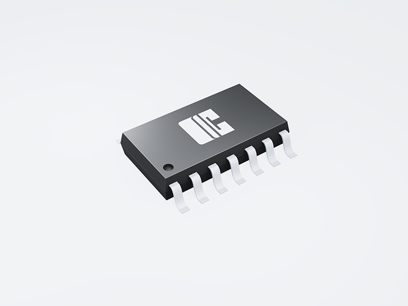
The AiP74HC/HCT04 is a hex inverter. The inputs include clamp diodes that enable the use of current limiting resistors to interface inputs to voltages in excess of VCC.
PN :
AiP74HC04Description :
Hex inverterVoltage Range :
2.0 - 6.0Nr of pins :
14Package :
DIP14/SOP14/TSSOP14Input levels:
For AiP74HC04: CMOS level
For AiP74HCT04: TTL level
Specified from -40℃ to +125℃
Packaging information: DIP14/SOP14/TSSOP14
-1769477122jv1iL1kpji.jpg)
-17694772923alulrrexR.jpg)
The AiP74HC/HCT196 is a presettable decade and binary counter. Output Q0 is connected to input CP1(—) for BCD count. Output Q3 is connected to input CP0(—) for bi-quinary count. In the counting modes, state changes are initiated by the falling edge of the clock.
Details-1769561865c92qFRf2EX.jpg)
The AiP74HC/HCT196 is a presettable decade and binary counter. Output Q0 is connected to input CP1(—) for BCD count. Output Q3 is connected to input CP0(—) for bi-quinary count. In the counting modes, state changes are initiated by the falling edge of the clock.
Details-17695651472X0l1ZKkjw.jpg)
The AiP74HC/HCT240 is an 8-bit inverting buffer/line driver with 3-state outputs. The device can be used as two 4-bit buffers or one 8-bit buffer. The device features two output enables (1OE(—) and 2OE(—)), each controlling four of the 3-state outputs. A HIGH on nOE(—) causes the outputs to assume a high-impedance OFF-state. Inputs include clamp diodes that enable the use of current limiting resistors to interface inputs to voltages in excess of VCC
Details-1769565273c5wHTNtUYA.jpg)
The AiP74HC/HCT240 is an 8-bit inverting buffer/line driver with 3-state outputs. The device can be used as two 4-bit buffers or one 8-bit buffer. The device features two output enables (1OE(—) and 2OE(—)), each controlling four of the 3-state outputs. A HIGH on nOE(—) causes the outputs to assume a high-impedance OFF-state. Inputs include clamp diodes that enable the use of current limiting resistors to interface inputs to voltages in excess of VCC.
Details-1769566649Hjv3Ld3Ug8.jpg)
The AiP74HC/HCT241 is an 8-bit buffer/line driver with 3-state outputs. The device can be used as two 4-bit buffers or one 8-bit buffer. The device features two output enables (1OE(—) and 2OE), each controlling four of the 3-state outputs. A HIGH on 1OE(—) or LOW on 2OE causes the associated outputs to assume a high-impedance OFF-state. Inputs include clamp diodes. This enables the use of current limiting resistors to interface inputs to voltages in excess of VCC. The AiP74HC/HCT241 device features reduced input threshold levels to allow interfacing to TTL logic levels.
Details-1769566724eNN8rnmjcg.jpg)
The AiP74HC/HCT241 is an 8-bit buffer/line driver with 3-state outputs. The device can be used as two 4-bit buffers or one 8-bit buffer. The device features two output enables (1OE(—) and 2OE), each controlling four of the 3-state outputs. A HIGH on 1OE(—) or LOW on 2OE causes the associated outputs to assume a high-impedance OFF-state. Inputs include clamp diodes. This enables the use of current limiting resistors to interface inputs to voltages in excess of VCC. The AiP74HC/HCT241 device features reduced input threshold levels to allow interfacing to TTL logic levels.
Details-1769567103SsK0oyxbSC.jpg)
The AiP74HC/HCT243 are quad bus transceivers featuring non-inverting 3-state bus compatible outputs in both send and receive directions. They are designed for 4-line asynchronous 2-way data communications between data buses. The output enable inputs (OE(—)A and OEB) can be used to isolate the buses.
Details-17695672826qDdUSaZJ5.jpg)
The AiP74HC/HCT243 are quad bus transceivers featuring non-inverting 3-state bus compatible outputs in both send and receive directions. They are designed for 4-line asynchronous 2-way data communications between data buses. The output enable inputs (OE(—)A and OEB) can be used to isolate the buses.
Details-1769580684JlE5FmyPtH.jpg)
The AiP74HC/HCT244 is an 8-bit buffer/line driver with 3-state outputs. The device can be used as two 4-bit buffers or one 8-bit buffer. The device features two output enables (1OE(—) and 2OE(—)), each controlling four of the 3-state outputs. A HIGH on nOE(—) causes the outputs to assume a high-impedance OFF-state. Inputs include clamp diodes that enable the use of current limiting resistors to interface inputs to voltages in excess of VCC.
Details-1769580769K3ENbayJ48.jpg)
The AiP74HC/HCT244 is an 8-bit buffer/line driver with 3-state outputs. The device can be used as two 4-bit buffers or one 8-bit buffer. The device features two output enables (1OE(—) and 2OE(—)), each controlling four of the 3-state outputs. A HIGH on nOE(—) causes the outputs to assume a high-impedance OFF-state. Inputs include clamp diodes that enable the use of current limiting resistors to interface inputs to voltages in excess of VCC.
Details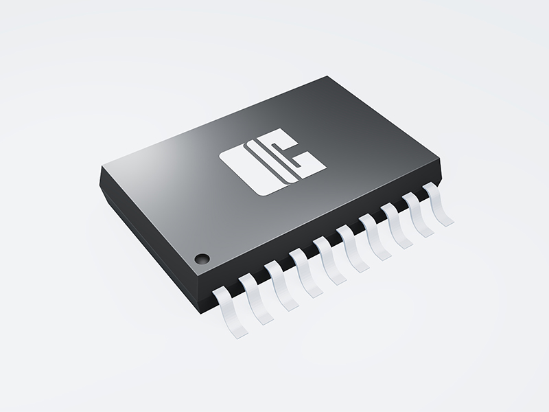
The AiP74HC245 is an 8-bit transceiver with 3-state outputs. The device features an output enable (OE — ) and send/receive (DIR) for direction control. A HIGH on (OE —)causes the outputs to assume ahigh-impedance OFF-state. Inputs include clamp diodes. This enables the use of current limiting resistors to interface inputs to voltages in excess of VCC
Details-1769580927USpKelMtOh.jpg)
The AiP74HC/HCT247 feature active-low outputs designed for driving common-anode LEDs or incandescent indicators directly. Display patterns for BCD input counts above 9 are unique symbols to authenticate input conditions.
Details
The AiP74HCT245 is an 8-bit transceiver with 3-state outputs. The device features an output enable (OE — ) and send/receive (DIR) for direction control.
Details-1769581396d02IDWKiNO.jpg)
The AiP74HC/HCT248 feature active-low outputs designed for driving common-cathode LEDs or incandescent indicators directly. Display patterns for BCD input counts above 9 are unique symbols to authenticate input conditions.
Details
The AiP74HC138 decodes three binary weighted address inputs(A0, A1 and A2) to eight mutually exclusive outputs (Y(—)0 to Y(—)7).
Details-1769581517LXS5QhMDcc.jpg)
The AiP74HC/HCT251 is an 8-bit multiplexer with eight binary inputs (I0 to I7), three select inputs (S0 to S2) and an output enable input (OE(—)). The select inputs select one of the eight binary inputs and route it to the complementary outputs (Y and Y(—)). A HIGH on OE(—) causes the outputs to assume a high-impedance OFF-state. Inputs include clamp diodes that enable the use of current limiting resistors to interface inputs to voltages in excess of VCC.
Details
The AiP74HCT138 decodes three binary weighted address inputs(A0, A1 and A2) to eight mutually exclusive outputs (Y(—)0 to Y(—)7).
Details-17695817539bWrX6JSIL.jpg)
The AiP74HC/HCT251 is an 8-bit multiplexer with eight binary inputs (I0 to I7), three select inputs (S0 to S2) and an output enable input (OE(—)). The select inputs select one of the eight binary inputs and route it to the complementary outputs (Y and Y(—)). A HIGH on OE(—) causes the outputs to assume a high-impedance OFF-state. Inputs include clamp diodes that enable the use of current limiting resistors to interface inputs to voltages in excess of VCC.
Details
-17695828134yuhMBvsAP.jpg)
The AiP74HC/HCT259 is an 8-bit addressable latch. The device features four modes of operation. In the addressable latch mode, data on the D input is written into the latch addressed by the inputs A0 to A3. The addressed latch will follow the data input, non-addressed latches will retain their previous states. In memory mode, all latches retain their previous states and are unaffected by the data or address inputs. In the 3-to-8 decoding or demultiplexing mode, the addressed output follows the D input and all other outputs are LOW. In the reset mode, all outputs are forced LOW and unaffected by the data or address inputs. Inputs include clamp diodes. This enables the use of current limiting resistors to interface inputs to voltages in excess of VCC.
Details
-1769583039uoKphYEKUM.jpg)
The AiP74HC/HCT259 is an 8-bit addressable latch. The device features four modes of operation. In the addressable latch mode, data on the D input is written into the latch addressed by the inputs A0 to A3. The addressed latch will follow the data input, non-addressed latches will retain their previous states. In memory mode, all latches retain their previous states and are unaffected by the data or address inputs. In the 3-to-8 decoding or demultiplexing mode, the addressed output follows the D input and all other outputs are LOW. In the reset mode, all outputs are forced LOW and unaffected by the data or address inputs. Inputs include clamp diodes. This enables the use of current limiting resistors to interface inputs to voltages in excess of VCC.
Details-1769588143JEbaD36zeV.jpg)
The AiP74HC/HCT266 contains four independent 2-input XNOR Gates with open-drain outputs
Details
-1769588224qNmEV3D0Em.jpg)
The AiP74HC/HCT266 contains four independent 2-input XNOR Gates with open-drain outputs
Details
-1769588337DfFRMq62mq.jpg)
The AiP74HC/HCT273 is an octal positive-edge triggered D-type flip-flop. The device features clock (CP) and master reset (MR(—)) inputs. The outputs Qn will assume the state of their corresponding Dn inputs that meet the set-up and hold time requirements on the LOW-to-HIGH clock (CP) transition. A LOW on MR(—) forces the outputs LOW independently of clock and data inputs. Inputs include clamp diodes. This enables the use of current limiting resistors to interface inputs to voltages in excess of VCC.
Details
-1769588427hLq11mzSQO.jpg)
The AiP74HC/HCT273 is an octal positive-edge triggered D-type flip-flop. The device features clock (CP) and master reset (MR(—)) inputs. The outputs Qn will assume the state of their corresponding Dn inputs that meet the set-up and hold time requirements on the LOW-to-HIGH clock (CP) transition. A LOW on MR(—) forces the outputs LOW independently of clock and data inputs. Inputs include clamp diodes. This enables the use of current limiting resistors to interface inputs to voltages in excess of VCC.
Details
The AiP74HCT123 are high-speed Si-gate CMOS devices and are pin compatible with Low-power Schottky TTL (LSTTL).
Details-1769588560N4RhJlBrQa.jpg)

The AiP74HC123 are high-speed Si-gate CMOS devices and are pin compatible with Low-power Schottky TTL (LSTTL).
Details-1769588664udNSattNrA.jpg)

The AiP74HC125 is a quad buffer/line driver with 3-state outputs controlled by the output enable inputs (nOE(—)).
Details-1769588807i1sTBUUs1A.jpg)
The AiP74HC/HCT280 is a 9-bit parity generator or checker. Both even and odd parity outputs are available. The even parity output (PE) is HIGH when an even number of data inputs (I0 to I8) is HIGH. The odd parity output (PO) is HIGH when an odd number of data inputs are HIGH. Expansion to larger word sizes is accomplished by tying the even outputs (PE) of up to nine parallel devices to the final stage data inputs. Inputs include clamp diodes. It enables the use of current limiting resistors to interface inputs to voltages in excess of VCC.
Details
The AiP74HCT125 is a quad buffer/line driver with 3-state outputs controlled by the output enable inputs (nOE(—)).
Details-1769588968uMA3dyeXqw.jpg)
The AiP74HC/HCT280 is a 9-bit parity generator or checker. Both even and odd parity outputs are available. The even parity output (PE) is HIGH when an even number of data inputs (I0 to I8) is HIGH. The odd parity output (PO) is HIGH when an odd number of data inputs are HIGH. Expansion to larger word sizes is accomplished by tying the even outputs (PE) of up to nine parallel devices to the final stage data inputs. Inputs include clamp diodes. It enables the use of current limiting resistors to interface inputs to voltages in excess of VCC.
Details
The AiP74HC390 is a dual 4-bit decade ripple counter divided into four separately clocked sections.
Details-17695891743DCQjx0JnJ.jpg)
The AiP74HC/HCT283 adds two 4-bit binary words (An plus Bn) plus the incoming carry (CIN). The binary sum appears on the sum outputs (S1 to S4) and the out-going carry (COUT) according to the equation: CIN+(A1+B1)+2(A2+B2)+4(A3+B3)+8(A4+B4)==S1+2S2+4S3+8S4+16COUT Where (+) = plus. Due to the symmetry of the binary add function, the AiP74HC/HCT283 can be used with either all active HIGH operands (positive logic) or all active LOW operands (negative logic). In case of all active LOW operands the results S1 to S4 and COUT should be interpreted also as active LOW. With active HIGH inputs, CIN must be held LOW when no carry in is intended. Interchanging inputs of equal weight does not affect the operation, thus CIN, A1, B1 can be assigned arbitrarily to pins 5, 6, 7, etc.
Details
The AiP74HCT390 is a dual 4-bit decade ripple counter divided into four separately clocked sections.
Details-1769589272kF6YGhBXse.jpg)
The AiP74HC/HCT283 adds two 4-bit binary words (An plus Bn) plus the incoming carry (CIN). The binary sum appears on the sum outputs (S1 to S4) and the out-going carry (COUT) according to the equation: CIN+(A1+B1)+2(A2+B2)+4(A3+B3)+8(A4+B4)==S1+2S2+4S3+8S4+16COUT Where (+) = plus. Due to the symmetry of the binary add function, the AiP74HC/HCT283 can be used with either all active HIGH operands (positive logic) or all active LOW operands (negative logic). In case of all active LOW operands the results S1 to S4 and COUT should be interpreted also as active LOW. With active HIGH inputs, CIN must be held LOW when no carry in is intended. Interchanging inputs of equal weight does not affect the operation, thus CIN, A1, B1 can be assigned arbitrarily to pins 5, 6, 7, etc.
Details
The AiP74HC157 are quad 2-input multiplexers which select 4 bits of data from two sources under the control of a common data select input (S).
Details-1769589411n7oKPkI9RN.jpg)
The AiP74HC/HCT365 is a hex buffer/line driver with 3-state outputs controlled by the output enable inputs (OE(—)n). A HIGH on OE(—)n causes the outputs to assume a high impedance OFF-state. Inputs include clamp diodes. This enables the use of current limiting resistors to interface inputs to voltages in excess of VCC.
Details
The AiP74HCT157 are quad 2-input multiplexers which select 4 bits of data from two sources under the control of a common data select input (S).
Details-1769589498DNQMdughcL.jpg)
The AiP74HC/HCT365 is a hex buffer/line driver with 3-state outputs controlled by the output enable inputs (OE(—)n). A HIGH on OE(—)n causes the outputs to assume a high impedance OFF-state. Inputs include clamp diodes. This enables the use of current limiting resistors to interface inputs to voltages in excess of VCC.
Details
The AiP74HC164 is an 8-bit serial-in/parallel-out shift register. e AiP74HC/HCT164 is an 8-bit serial-in/parallel-out shift register. The device features two serial dataThe AiP74HC/HCT164 is an 8-bit serial-in/parallel-out shift register. The device features two serial data inputs (DSA and DSB), eight parallel data outputs (Q0 to Q7). inputs (DSA and DSB), eight parallel data outputs (Q0 to Q7).
Details-1769661600fcHl8bBOZv.jpg)
The AiP74HC/HCT366 is a hex inverting buffer/line driver with 3-state outputs controlled by the output enable inputs (OE(—)n). A HIGH on OE(—)n causes the outputs to assume a high impedance OFF-state. Inputs include clamp diodes. This enables the use of current limiting resistors to interface inputs to voltages in excess of VCC.
Details
-1769661665IzSFDEeSEW.jpg)
The AiP74HC/HCT366 is a hex inverting buffer/line driver with 3-state outputs controlled by the output enable inputs (OE(—)n). A HIGH on OE(—)n causes the outputs to assume a high impedance OFF-state. Inputs include clamp diodes. This enables the use of current limiting resistors to interface inputs to voltages in excess of VCC.
Details-1769661812uVo0ixlIjn.jpg)
The AiP74HC/HCT367 is a hex buffer/line driver with 3-state outputs controlled by the output enable inputs (nOE(—)). A HIGH on nOE(—) causes the outputs to assume a high impedance OFF-state. Inputs include clamp diodes. This enables the use of current limiting resistors to interface inputs to voltages in excess of VCC.
Details-1769661886g7lAkpry5r.jpg)
The AiP74HC/HCT367 is a hex buffer/line driver with 3-state outputs controlled by the output enable inputs (nOE(—)). A HIGH on nOE(—) causes the outputs to assume a high impedance OFF-state. Inputs include clamp diodes. This enables the use of current limiting resistors to interface inputs to voltages in excess of VCC.
Details
The AiP74HC/HCT237 is a 3-to-8 line decoder, demultiplexer with latches at the three address inputs (An).
Details-1769662011afD5EIQjx7.jpg)
The AiP74HC/HCT373 is an octal D-type transparent latch with 3-state outputs. The device features latch enable (LE) and output enable (OE(—)) inputs. When LE is HIGH, data at the inputs enter the latches. In this condition the latches are transparent, a latch output will change each time its corresponding D-input changes. When LE is LOW the latches store the information that was present at the inputs a set-up time preceding the HIGH-to-LOW transition of LE. A HIGH on OE(—) causes the outputs to assume a high-impedance OFF-state. Operation of the OE(—) input does not affect the state of the latches. Inputs include clamp diodes. This enables the use of current limiting resistors to interface inputs to voltages in excess of VCC.
Details
The AiP74HCT237 is a 3-to-8 line decoder, demultiplexer with latches at the three address inputs (An).
Details-17696620848rQMTSEl4A.jpg)
The AiP74HC/HCT373 is an octal D-type transparent latch with 3-state outputs. The device features latch enable (LE) and output enable (OE(—)) inputs. When LE is HIGH, data at the inputs enter the latches. In this condition the latches are transparent, a latch output will change each time its corresponding D-input changes. When LE is LOW the latches store the information that was present at the inputs a set-up time preceding the HIGH-to-LOW transition of LE. A HIGH on OE(—) causes the outputs to assume a high-impedance OFF-state. Operation of the OE(—) input does not affect the state of the latches. Inputs include clamp diodes. This enables the use of current limiting resistors to interface inputs to voltages in excess of VCC.
Details
The AiP74HC/HCT238 decodes three binary weighted address inputs (A0, A1 and A2) to eight mutually exclusive outputs (Y0 to Y7).
Details-1769662189tByqUd3ba6.jpg)
The AiP74HC/HCT374 is an octal positive-edge triggered D-type flip-flop with 3-state outputs. The device features a clock (CP) and output enable (OE(—)) inputs. The flip-flops will store the state of their individual D-inputs that meet the set-up and hold time requirements on the LOW-to-HIGH clock (CP) transition. A HIGH on OE(—) causes the outputs to assume a high-impedance OFF-state. Operation of the OE(—) input does not affect the state of the flip-flops. Inputs also include clamp diodes, this enables the use of current limiting resistors to interface inputs to voltages in excess of VCC. The AiP74HCT374 features reduced input threshold levels to allow interfacing to TTL logic levels.
Details
The AiP74HC/HCT238 decodes three binary weighted address inputs (A0, A1 and A2) to eight mutually exclusive outputs (Y0 to Y7).
Details-17696622697EMzfG9dIn.jpg)
The AiP74HC/HCT374 is an octal positive-edge triggered D-type flip-flop with 3-state outputs. The device features a clock (CP) and output enable (OE(—)) inputs. The flip-flops will store the state of their individual D-inputs that meet the set-up and hold time requirements on the LOW-to-HIGH clock (CP) transition. A HIGH on OE(—) causes the outputs to assume a high-impedance OFF-state. Operation of the OE(—) input does not affect the state of the flip-flops. Inputs also include clamp diodes, this enables the use of current limiting resistors to interface inputs to voltages in excess of VCC. The AiP74HCT374 features reduced input threshold levels to allow interfacing to TTL logic levels.
Details
-1769662412SG4QV6cdsI.jpg)

-1769662474Aom47PAeLF.jpg)
-1769750250nL9pwru2P8.jpg)
The AiP74HC/HCT540 is an 8-bit inverting buffer/line driver with 3-state outputs. The device features two output enables (OE(—)1 and OE(—)2). A HIGH on OE(—)n causes the outputs to assume a high-impedance OFF-state. Inputs include clamp diodes. This enables the use of current limiting resistors to interface inputs to voltages in excess of VCC.
Details-1769750319bwzB0cyHnT.jpg)
The AiP74HC/HCT540 is an 8-bit inverting buffer/line driver with 3-state outputs. The device features two output enables (OE(—)1 and OE(—)2). A HIGH on OE(—)n causes the outputs to assume a high-impedance OFF-state. Inputs include clamp diodes. This enables the use of current limiting resistors to interface inputs to voltages in excess of VCC.
Details-17697526006OGygh48Qd.jpg)
The AiP74HC/HCT541 is an octal non-inverting buffer/line driver with 3-state outputs. The device features two output enables (OE(—)1 and OE(—)2). A HIGH on OE(—)n causes the outputs to assume a high-impedance OFF-state. Inputs include clamp diodes that enable the use of current limiting resistors to interface inputs to voltages in excess of VCC.
Details-1769752677Y3NMkHUdsL.jpg)
The AiP74HC/HCT541 is an octal non-inverting buffer/line driver with 3-state outputs. The device features two output enables (OE(—)1 and OE(—)2). A HIGH on OE(—)n causes the outputs to assume a high-impedance OFF-state. Inputs include clamp diodes that enable the use of current limiting resistors to interface inputs to voltages in excess of VCC.
Details-1769756121c2UdSoFC7Z.jpg)
The AiP74HC/HCT563 is an 8-bit D-type transparent latch with 3-state inverting outputs. The device features latch enable (LE) and output enable (OE(—)) inputs. When LE is HIGH, data at the inputs enter the latches. In this condition the latches are transparent, a latch output will change each time its corresponding D-input changes. When LE is LOW the latches store the information that was present at the inputs a set-up time preceding the HIGH-to-LOW transition of LE. A HIGH on OE(—) causes the outputs to assume a high-impedance OFF-state. Operation of the OE(—) input does not affect the state of the latches. Inputs include clamp diodes. This enables the use of current limiting resistors to interface inputs to voltages in excess of VCC.
Details-1769756259xxXr90d7Km.jpg)
The AiP74HC/HCT563 is an 8-bit D-type transparent latch with 3-state inverting outputs. The device features latch enable (LE) and output enable (OE(—)) inputs. When LE is HIGH, data at the inputs enter the latches. In this condition the latches are transparent, a latch output will change each time its corresponding D-input changes. When LE is LOW the latches store the information that was present at the inputs a set-up time preceding the HIGH-to-LOW transition of LE. A HIGH on OE(—) causes the outputs to assume a high-impedance OFF-state. Operation of the OE(—) input does not affect the state of the latches. Inputs include clamp diodes. This enables the use of current limiting resistors to interface inputs to voltages in excess of VCC.
Details-1769756394JIl6iyoRRe.jpg)
The AiP74HC/HCT573 is an 8-bit D-type transparent latch with 3-state outputs. The device features latch enable (LE) and output enable (OE(—)) inputs. When LE is HIGH, data at the inputs enter the latches. In this condition the latches are transparent, a latch output will change each time its corresponding D-input changes. When LE is LOW the latches store the information that was present at the inputs a set-up time preceding the HIGH-to-LOW transition of LE. A HIGH on OE(—) causes the outputs to assume a high-impedance OFF-state. Operation of the OE(—) input does not affect the state of the latches. Inputs include clamp diodes. This enables the use of current limiting resistors to interface inputs to voltages in excess of VCC.
Details-1769756418LjKauSIzzQ.jpg)
The AiP74HC/HCT573 is an 8-bit D-type transparent latch with 3-state outputs. The device features latch enable (LE) and output enable (OE(—)) inputs. When LE is HIGH, data at the inputs enter the latches. In this condition the latches are transparent, a latch output will change each time its corresponding D-input changes. When LE is LOW the latches store the information that was present at the inputs a set-up time preceding the HIGH-to-LOW transition of LE. A HIGH on OE(—) causes the outputs to assume a high-impedance OFF-state. Operation of the OE(—) input does not affect the state of the latches. Inputs include clamp diodes. This enables the use of current limiting resistors to interface inputs to voltages in excess of VCC.
Details-17697565833Qz9pWJp7P.jpg)
The AiP74HC/HCT574 is an octal positive-edge triggered D-type flip-flop with 3-state outputs. The device features a clock (CP) and output enable (OE(—)) inputs. A HIGH on OE(—) causes the outputs to assume a high-impedance OFF-state. Operation of the OE(—) input does not affect the state of the flip-flops.
Details-1770007749QNEudGVXkH.jpg)
The AiP74HC/HCT574 is an octal positive-edge triggered D-type flip-flop with 3-state outputs. The device features a clock (CP) and output enable (OE(—)) inputs. A HIGH on OE(—) causes the outputs to assume a high-impedance OFF-state. Operation of the OE(—) input does not affect the state of the flip-flops.
Details-1770007916vsslLHHD2L.jpg)
The AiP74HC589 device consists of an 8−bit storage latch which feeds parallel data to an 8−bit shift register.Inputs include clamp diodes. It enables the use of current limiting resistors to interface inputs to voltages in excess of VCC.
Details-1770008115bRth9F2Z98.jpg)
The 74HC594/74HCT594 is an 8-bit serial-in/serial or parallel-out shift register with a storage register.
Details-1770684374FYNjVLEjp4.jpg)
The AiP74HC/HCT595 is an 8-bit serial-in/serial or parallel-out shift register with a storage register and 3-state outputs. Both the shift and storage register have separate clocks. The device features a serial input (DS) and a serial output (Q7S) to enable cascading and an asynchronous reset MR(—) input. A LOW on MR(—) will reset the shift register. Data is shifted on the LOW-to-HIGH transitions of the SHCP input. The data in the shift register is transferred to the storage register on a LOW-to-HIGH transition of the STCP input. If both clocks are connected together, the shift register will always be one clock pulse ahead of the storage register. Data in the storage register appears at the output whenever the output enable input (OE(—)) is LOW. A HIGH on OE(—) causes the outputs to assume a high-impedance OFF-state. Operation of the OE(—) input does not affect the state of the registers. Inputs include clamp diodes. This enables the use of current limiting resistors to interface inputs to voltages in excess of VCC.
Details-1775528686UgLycuZTdX.jpg)
The AIP74HC4017 is a 5-stage Johnson decade counter with ten spike-free decoded active HIGH outputs (Q0 to Q9), an active LOW carry output from the most significant flip-flop (Q5-9), active HIGH and active LOW clock inputs (CP0, CP—1) and an overriding asynchronous master reset input (MR)
Details-1775529655JWt5PiWpjE.jpg)
The AiP74HC4040/HCT4040 is a 12-stage binary ripple counter with a clock input ( CP ), an overriding asynchronous master reset input (MR) and twelve parallel outputs (Q0 to Q11). Inputs include clamp diodes that enable the use of current limiting resistors to interface inputs to voltages in excess of VCC.
Details-1775530363dDjNm5Iqdy.jpg)
The AiP74HC4040/HCT4040 is a 12-stage binary ripple counter with a clock input ( CP ), an overriding asynchronous master reset input (MR) and twelve parallel outputs (Q0 to Q11). Inputs include clamp diodes that enable the use of current limiting resistors to interface inputs to voltages in excess of VCC.
Details-1775530757UYla7ZSRy9.jpg)
The AiP74HC/HCT7266 provide the exclusive-nor function with active push-pull output. Inputs include clamp diodes. This enables the use of current limiting resistors to interface inputs to voltages in excess of VCC.
Details-1775530830hanS87FZRH.jpg)
The AiP74HC/HCT7266 provide the exclusive-nor function with active push-pull output. Inputs include clamp diodes. This enables the use of current limiting resistors to interface inputs to voltages in excess of VCC.
Details-1775531080Onh2qvonYe.jpg)
The AiP74HC/HCT40103 is an 8-bit synchronous down counter. It has control inputs for enabling or disabling the clock (CP), for clearing the counter to its maximum count and for presetting the counter either synchronously or asynchronously. In normal operation, the counter is decremented by one count on each positive-going transition of the clock (CP). Counting is inhibited when the terminal enable input ( ) is HIGH. The terminal count output ( ) goes LOW when the count reaches zero if is LOW, and remains LOW for one full clock period. When the synchronous preset enable input ( ) is LOW, data at the jam input (P0 to P7) is clocked into the counter on the next positive-going clock transition regardless of the state of . When the asynchronous preset enable input ( ) is LOW, data at the jam input (P0 to P7) is asynchronously forced into the counter regardless of the state of , , or CP. The jam inputs (P0 to P7) represent a single 8-bit binary word. When the master reset input ( ) is LOW, the counter is asynchronously cleared to its maximum count (decimal 255) regardless of the state of any other input. If all control inputs except are HIGH at the time of zero count, the counters will jump to the maximum count, giving a counting sequence of 256 clock pulses long. Device may be cascaded using the input and the TC output, in either a synchronous or ripple mode. Inputs include clamp diodes. This enables the use of current limiting resistors to interface inputs to voltages in excess of VCC.
Details-1775531175MYPmnd9krd.jpg)
The AiP74HC/HCT40103 is an 8-bit synchronous down counter. It has control inputs for enabling or disabling the clock (CP), for clearing the counter to its maximum count and for presetting the counter either synchronously or asynchronously. In normal operation, the counter is decremented by one count on each positive-going transition of the clock (CP). Counting is inhibited when the terminal enable input ( ) is HIGH. The terminal count output ( ) goes LOW when the count reaches zero if is LOW, and remains LOW for one full clock period. When the synchronous preset enable input ( ) is LOW, data at the jam input (P0 to P7) is clocked into the counter on the next positive-going clock transition regardless of the state of . When the asynchronous preset enable input ( ) is LOW, data at the jam input (P0 to P7) is asynchronously forced into the counter regardless of the state of , , or CP. The jam inputs (P0 to P7) represent a single 8-bit binary word. When the master reset input ( ) is LOW, the counter is asynchronously cleared to its maximum count (decimal 255) regardless of the state of any other input. If all control inputs except are HIGH at the time of zero count, the counters will jump to the maximum count, giving a counting sequence of 256 clock pulses long. Device may be cascaded using the input and the TC output, in either a synchronous or ripple mode. Inputs include clamp diodes. This enables the use of current limiting resistors to interface inputs to voltages in excess of VCC.
Details
The AiP74HC1G126 and AiP74HCT1G126 is a non-inverting buffer/line driver with 3-state output.
Details-17683533067J83N1Yaoc.jpg)
The AiP74HC/HCT00 is a quad 2-input NAND gate. Inputs include clamp diodes. This enables the use of current limiting resistors to interface inputs to voltages in excess of VCC.
Details-17683537257zyYKGiSFt.jpg)
The AiP74HC/HCT01 contains four independent 2-input NAND Gates with open-drain outputs.
Details-1768353984tqxxtPGPxh.jpg)
The AiP74HC/HCT03 is a quad 2-input NAND gate with open-drain outputs. Inputs include clamp diodes. This enables the use of current limiting resistors to interface inputs to voltages in excess of VCC.
Details-17683558587zP7GEI6Ga.jpg)
The AiP74HC/HCT04 is a hex inverter. The inputs include clamp diodes that enable the use of current limiting resistors to interface inputs to voltages in excess of VCC.
Details-1768356727gxIyzUSxbx.jpg)
The AiP74HC/HCT05 contains six inverters. The outputs of the AiP74HC/HCT05 are open-drain and can be connected to other open-drain outputs to implement active-LOW wired-OR or active-HIGH wired-AND functions. The open-drain outputs require pull-up resistors to perform correctly.
Details-1768357960UO2aoj49ym.jpg)
The AiP74HC/HCT07 contains six buffers. The outputs of the AiP74HC/HCT07 are open-drain and can be connected to other open-drain outputs to implement active-LOW wired-OR or active-HIGH wired-AND functions. The open-drain outputs require pull-up resistors to perform correctly.
Details-1768358282d40GY1Ca7s.jpg)
The AiP74HC/HCT08 is a quad 2-input AND gate. Inputs include clamp diodes. This enables the use of current limiting resistors to interface inputs to voltages in excess of VCC.
Details-1768358531ayHoPm4zuB.jpg)
The AiP74HC/HCT10 is a triple 3-input NAND gate. Inputs include clamp diodes. This enables the use of current limiting resistors to interface inputs to voltages in excess of VCC.
Details-1768358676LoPtzNJAU1.jpg)
The AiP74HC/HCT11 is a triple 3-input AND gate. Inputs include clamp diodes. This enables the use of current limiting resistors to interface inputs to voltages in excess of VCC.Input levels: For AiP74HC11: CMOS level For AiP74HCT11: TTL level Specified from -40℃ to +125℃ Packaging information: DIP14/SOP14/TSSOP14
Details-1768358817o3cQrMaqKt.jpg)
The AiP74HC/HCT11 is a triple 3-input AND gate. Inputs include clamp diodes. This enables the use of current limiting resistors to interface inputs to voltages in excess of VCC.
Details-1768359162ZZme0XbO8N.jpg)
-1768359537rwYID2q2o2.jpg)
The AiP74HC/HCT14 is a hex inverter with Schmitt-trigger inputs. This device features reduced input threshold levels to allow interfacing to TTL logic levels. Inputs include clamp diodes. This enables the use of current limiting resistors to interface inputs to voltages in excess of VCC. Schmitt trigger inputs transform slowly changing input signals into sharply defined jitter-free output signals.
Details-17683595726K2LbjBxr9.jpg)
The AiP74HC/HCT14 is a hex inverter with Schmitt-trigger inputs. This device features reduced input threshold levels to allow interfacing to TTL logic levels. Inputs include clamp diodes. This enables the use of current limiting resistors to interface inputs to voltages in excess of VCC. Schmitt trigger inputs transform slowly changing input signals into sharply defined jitter-free output signals.
Details-1768373095XJQmm5th3l.jpg)
The AiP74HC/HCT20 is a dual 4-input NAND gate. Inputs include clamp diodes. This enables the use of current limiting resistors to interface inputs to voltages in excess of VCC.
Details-1768373381gVRBfUiEzT.jpg)
The AiP74HC/HCT21 provide the 4-input AND function. Inputs include clamp diodes. This enables the use of current limiting resistors to interface inputs to voltages in excess of VCC.
Details-1768373706d2qJWhItZe.jpg)
The AiP74HC/HCT27 is a triple 3-input NOR gate. Inputs include clamp diodes. This enables the use of current limiting resistors to interface inputs to voltages in excess of VCC.
Details-1768373944otIAgJyq3L.jpg)
The AiP74HC/HCT30 is an 8-input NAND gate. Inputs include clamp diodes. This enables the use of current limiting resistors to interface inputs to voltages in excess of VCC.
Details-1768378041YkrlUAhqUl.jpg)
The AiP74HC/HCT32 is a quad 2-input OR gate. Inputs include clamp diodes. This enables the use of current limiting resistors to interface inputs to voltages in excess of VCC.
Details-17683782558Q7swO2y5i.jpg)
The AiP74HC/HCT42 is a one of ten BCD to decimal decoder. It accepts four BCD inputs (0A to 3A) and provides ten mutually exclusive outputs (0Y(—) to 9Y(—)). The logic design ensures that all outputs are HIGH when binary codes greater than nine are applied to the inputs. The most significant input (3A) produces an useful inhibit function when the device is used as a 1-of-8 decoder. The 3A input can also be used as the data input in an 8-output demultiplexer application. Inputs include clamp diodes. This enables the use of current limiting resistors to interface inputs to voltages in excess of VCC.
Details-1768378354k2CehrbcJR.jpg)
The AiP74HC/HCT42 is a one of ten BCD to decimal decoder. It accepts four BCD inputs (0A to 3A) and provides ten mutually exclusive outputs (0Y(—) to 9Y(—)). The logic design ensures that all outputs are HIGH when binary codes greater than nine are applied to the inputs. The most significant input (3A) produces an useful inhibit function when the device is used as a 1-of-8 decoder. The 3A input can also be used as the data input in an 8-output demultiplexer application. Inputs include clamp diodes. This enables the use of current limiting resistors to interface inputs to voltages in excess of VCC.
Details-1768378858JJo9D1yBPN.jpg)
The AiP74HC/HCT73 is dual negative-edge triggered JK-type flip-flops featuring individual J, K, clock (nCP(—)) and reset (nR(—)) inputs; also complementary Q and Q(—) outputs.
Details-1768379032JU5ZbXPoTR.jpg)
The AiP74HC/HCT74 are dual positive edge triggered D-type flip-flop. They have individual data (nD), clock (nCP), set (nS(—)D) and reset (nR(—)D) inputs, and complementary nQ and nQ(—) outputs. Data at the nD-input, that meets the set-up and hold time requirements on the LOW-to-HIGH clock transition, is stored in the flip-flop and appears at the nQ output. Schmitt-trigger action in the clock input, makes the circuit highly tolerant to slower clock rise and fall times. Inputs include clamp diodes. This enables the use of current limiting resistors to interface inputs to voltages in excess of VCC.
Details-1768379146W9c41dArmY.jpg)
The AiP74HC/HCT74 are dual positive edge triggered D-type flip-flop. They have individual data (nD), clock (nCP), set (nS(—)D) and reset (nR(—)D) inputs, and complementary nQ and nQ(—) outputs. Data at the nD-input, that meets the set-up and hold time requirements on the LOW-to-HIGH clock transition, is stored in the flip-flop and appears at the nQ output. Schmitt-trigger action in the clock input, makes the circuit highly tolerant to slower clock rise and fall times. Inputs include clamp diodes. This enables the use of current limiting resistors to interface inputs to voltages in excess of VCC.
Details-1768379373PTF6uckear.jpg)
-1768379533so7ioSeeeB.jpg)
The AiP74HC/HCT85 is a 4-bit magnitude comparator that can be expanded to almost any length. They perform comparison of two 4-bit binary, BCD or other monotonic codes and present the three possible magnitude results at the outputs (QA>B, QA=B and QA<B). The 4-bit inputs are weighted (A0 to A3 and B0 to B3), where A3 and B3 are the most significant bits. For proper compare operation the expander inputs (IA>B, IA=B and IA<B) to the least significant position must be connected as follows: IA<B=IA>B=LOW and IA=B=HIGH. For words greater than 4-bits, units can be cascaded by connecting outputs QA>B, QA=B and QA
Details-1768379641pdC4cGuKwT.jpg)
The AiP74HC/HCT85 is a 4-bit magnitude comparator that can be expanded to almost any length. They perform comparison of two 4-bit binary, BCD or other monotonic codes and present the three possible magnitude results at the outputs (QA>B, QA=B and QA<B). The 4-bit inputs are weighted (A0 to A3 and B0 to B3), where A3 and B3 are the most significant bits. For proper compare operation the expander inputs (IA>B, IA=B and IA<B) to the least significant position must be connected as follows: IA<B=IA>B=LOW and IA=B=HIGH. For words greater than 4-bits, units can be cascaded by connecting outputs QA>B, QA=B and QA
Details-1768379871PWi67JGf6H.jpg)
The AiP74HC/HCT86 is a quad 2-input EXCLUSIVE-OR gate. Inputs include clamp diodes. This enables the use of current limiting resistors to interface inputs to voltages in excess of VCC.
Details-17689713086IXFIYYxUb.jpg)
-1768971585VcwcKUjdj5.jpg)
-1768971715q3bQGXLxgD.jpg)
The AiP74HC/HCT107 is dual negative-edge triggered JK-type flip-flops featuring individual J, K, clock (nCP(—)) and reset (nR(—)) inputs; also complementary Q and Q(—) outputs.
Details-1768971812z9HLq4RiPM.jpg)
The AiP74HC/HCT107 is dual negative-edge triggered JK-type flip-flops featuring individual J, K, clock (nCP(—)) and reset (nR(—)) inputs; also complementary Q and Q(—) outputs.
Details-1768971945xaV1WbBKyf.jpg)
-1768972006HdM0sODvuF.jpg)
-1768972179piNAU13gRy.jpg)
The AiP74HC/HCT126 is a quad buffer/line driver with 3-state outputs controlled by the output enable inputs (nOE). A LOW on nOE causes the outputs to assume a high-impedance OFF-state. Inputs include clamp diodes. This enables the use of current limiting resistors to interface inputs to voltages in excess of VCC.
Details-1768972311zXqvICEXDV.jpg)
The AiP74HC/HCT126 is a quad buffer/line driver with 3-state outputs controlled by the output enable inputs (nOE). A LOW on nOE causes the outputs to assume a high-impedance OFF-state. Inputs include clamp diodes. This enables the use of current limiting resistors to interface inputs to voltages in excess of VCC.
Details-1768972649Z60q88aaWs.jpg)
The AiP74HC/HCT132 is a quad 2-input NAND gate with Schmitt-trigger inputs. Inputs include clamp diodes. This enables the use of current limiting resistors to interface inputs to voltages in excess of VCC. Schmitt trigger inputs transform slowly changing input signals into sharply defined jitter-free output signals.
Details-1768972794atUcyWUy7N.jpg)
The AiP74HC/HCT132 is a quad 2-input NAND gate with Schmitt-trigger inputs. Inputs include clamp diodes. This enables the use of current limiting resistors to interface inputs to voltages in excess of VCC. Schmitt trigger inputs transform slowly changing input signals into sharply defined jitter-free output signals.
Details-1768972959ikWqjNmLh7.jpg)
The AiP74HC/HCT139 decodes two binary weighted address inputs (nA0, nA1) to four mutually exclusive outputs (nY(—)0 to nY(—)3). Each decoder features an enable input (nE(—)). When nE(—) is HIGH all outputs are forced HIGH. The enable input can be used as the data input for a 1-to-4 demultiplexer application. Inputs include clamp diodes. This enables the use of current limiting resistors to interface inputs to voltages in excess of VCC.
Details-1768973036SaSEAPMqw8.jpg)
The AiP74HC/HCT139 decodes two binary weighted address inputs (nA0, nA1) to four mutually exclusive outputs (nY(—)0 to nY(—)3). Each decoder features an enable input (nE(—)). When nE(—) is HIGH all outputs are forced HIGH. The enable input can be used as the data input for a 1-to-4 demultiplexer application. Inputs include clamp diodes. This enables the use of current limiting resistors to interface inputs to voltages in excess of VCC.
Details-1768973184zN6AcFhiYe.jpg)
-17689733489vfmTWR4BA.jpg)
-1768973479PA3P2ODOwt.jpg)
The AiP74HC/HCT147 9-input priority encoders accept data from nine active LOW inputs The devices provide the 10-line to 4-line priority encoding function by use of the implied decimal “zero”. The “zero” is encoded when all nine data inputs are HIGH, forcing all four outputs HIGH.
Details-1768973589IiiglbBAja.jpg)
The AiP74HC/HCT147 9-input priority encoders accept data from nine active LOW inputs The devices provide the 10-line to 4-line priority encoding function by use of the implied decimal “zero”. The “zero” is encoded when all nine data inputs are HIGH, forcing all four outputs HIGH.
Details-1768974076sNijlh39YZ.jpg)
The AiP74HC/HCT148 encodes eight data lines to three-line (4-2-1) binary (octal). Cascading circuitry (enable input EI and enable output EO) is provided to allow octal expansion without the need for external circuitry. The data inputs and outputs are active at the low logic level.
Details-1768974162XmIKg6vTQw.jpg)
The AiP74HC/HCT148 encodes eight data lines to three-line (4-2-1) binary (octal). Cascading circuitry (enable input EI and enable output EO) is provided to allow octal expansion without the need for external circuitry. The data inputs and outputs are active at the low logic level.
Details-176897432775vPNnRrvT.jpg)
The AiP74HC/HCT151 are 8-bit multiplexer with eight binary inputs (I0 to I7), three select inputs (S0 to S2) and an enable input (E(—)). One of the eight binary inputs is selected by the select inputs and routed to the complementary outputs (Y and Y(—)). A HIGH on E(—) forces the output Y LOW and output Y(—) HIGH. Inputs also include clamp diodes that enable the use of current limiting resistors to interface inputs to voltages in excess of VCC.
Details-1768974403ZMCKkyo0Bl.jpg)
The AiP74HC/HCT151 are 8-bit multiplexer with eight binary inputs (I0 to I7), three select inputs (S0 to S2) and an enable input (E(—)). One of the eight binary inputs is selected by the select inputs and routed to the complementary outputs (Y and Y(—)). A HIGH on E(—) forces the output Y LOW and output Y(—) HIGH. Inputs also include clamp diodes that enable the use of current limiting resistors to interface inputs to voltages in excess of VCC.
Details-17689744936VhtSrBYUL.jpg)
The AiP74HC/HCT153 is a dual 4-input multiplexer. The device features independent enable inputs (nE(—)) and common data select inputs (S0 and S1). For each multiplexer, the select inputs select one of the four binary inputs and routes it to the multiplexer output (nY). A HIGH on E(—) forces the corresponding multiplexer outputs LOW. Inputs include clamp diodes. This enables the use of current limiting resistors to interface inputs to voltages in excess of VCC.
Details-1768974587lJr1pC5Ke7.jpg)
The AiP74HC/HCT153 is a dual 4-input multiplexer. The device features independent enable inputs (nE(—)) and common data select inputs (S0 and S1). For each multiplexer, the select inputs select one of the four binary inputs and routes it to the multiplexer output (nY). A HIGH on E(—) forces the corresponding multiplexer outputs LOW. Inputs include clamp diodes. This enables the use of current limiting resistors to interface inputs to voltages in excess of VCC.
Details
-1768975768OtLfOBvx7l.jpg)
-17689758339Z0qOWHiT1.jpg)
-1768975976TRFd2x0nCP.jpg)
The AiP74HC/HCT160 is a synchronous presettable decade counter with an internal look-ahead carry. Synchronous operation is provided by having all flip-flops clocked simultaneously on the positive-going edge of the clock (CP). The outputs (Q0 to Q3) of the counters may be preset HIGH or LOW. A LOW at the parallel enable input (PE(—)) disables the counting action and causes the data at the data inputs (D0 to D3) to be loaded into the counter on the positive-going edge of the clock. Preset takes place regardless of the levels at count enable inputs (CEP and CET). A LOW at the master reset input (MR(—)) sets Q0 to Q3 LOW regardless of the levels at input pins CP, PE(—), CET and CEP (thus providing an asynchronous clear function). The look-ahead carry simplifies serial cascading of the counters. Both CEP and CET must be HIGH to count. The CET input is fed forward to enable the terminal count output (TC). The TC output thus enabled will produce a HIGH output pulse of a duration approximately equal to a HIGH output of Q0. This pulse can be used to enable the next cascaded stage. The maximum clock frequency for the cascaded counters is determined by the CP to TC propagation delay and CEP to CP set-up time, according to the following formula: fmax=1/(tP(max)(CP to TC)+tSU(CEP to CP)) Inputs include clamp diodes. This enables the use of current limiting resistors to interface inputs to voltages in excess of VCC.
Details-1768976043KcNUnBDRdL.jpg)
The AiP74HC/HCT160 is a synchronous presettable decade counter with an internal look-ahead carry. Synchronous operation is provided by having all flip-flops clocked simultaneously on the positive-going edge of the clock (CP). The outputs (Q0 to Q3) of the counters may be preset HIGH or LOW. A LOW at the parallel enable input (PE(—)) disables the counting action and causes the data at the data inputs (D0 to D3) to be loaded into the counter on the positive-going edge of the clock. Preset takes place regardless of the levels at count enable inputs (CEP and CET). A LOW at the master reset input (MR(—)) sets Q0 to Q3 LOW regardless of the levels at input pins CP, PE(—), CET and CEP (thus providing an asynchronous clear function). The look-ahead carry simplifies serial cascading of the counters. Both CEP and CET must be HIGH to count. The CET input is fed forward to enable the terminal count output (TC). The TC output thus enabled will produce a HIGH output pulse of a duration approximately equal to a HIGH output of Q0. This pulse can be used to enable the next cascaded stage. The maximum clock frequency for the cascaded counters is determined by the CP to TC propagation delay and CEP to CP set-up time, according to the following formula: fmax=1/(tP(max)(CP to TC)+tSU(CEP to CP)) Inputs include clamp diodes. This enables the use of current limiting resistors to interface inputs to voltages in excess of VCC.
Details-1768976178YfHCc0apOd.jpg)
The AiP74HC/HCT161 is a synchronous presettable binary counter with an internal look-head carry. Synchronous operation is provided by having all flip-flops clocked simultaneously on the positive-going edge of the clock (CP). The outputs (Q0 to Q3) of the counters may be preset HIGH or LOW. A LOW at the parallel enable input (PE(—)) disables the counting action and causes the data at the data inputs (D0 to D3) to be loaded into the counter on the positive-going edge of the clock. Preset takes place regardless of the levels at count enable inputs (CEP and CET). A LOW at the master reset input (MR(—)) sets Q0 to Q3 LOW regardless of the levels at input pins CP, PE(—), CET and CEP (thus providing an asynchronous clear function). The look-ahead carry simplifies serial cascading of the counters. Both CEP and CET must be HIGH to count. The CET input is fed forward to enable the terminal count output (TC). The TC output thus enabled will produce a HIGH output pulse of a duration approximately equal to a HIGH output of Q0. This pulse can be used to enable the next cascaded stage. The maximum clock frequency for the cascaded counters is determined by the CP to TC propagation delay and CEP to CP set-up time, according to the following formula: fmax=1/(tP(max)(CP to TC)+tSU(CEP to CP)) Inputs include clamp diodes. This enables the use of current limiting resistors to interface inputs to voltages in excess of VCC.
Details-1768976264cwql0khlwv.jpg)
The AiP74HC/HCT161 is a synchronous presettable binary counter with an internal look-head carry. Synchronous operation is provided by having all flip-flops clocked simultaneously on the positive-going edge of the clock (CP). The outputs (Q0 to Q3) of the counters may be preset HIGH or LOW. A LOW at the parallel enable input (PE(—)) disables the counting action and causes the data at the data inputs (D0 to D3) to be loaded into the counter on the positive-going edge of the clock. Preset takes place regardless of the levels at count enable inputs (CEP and CET). A LOW at the master reset input (MR(—)) sets Q0 to Q3 LOW regardless of the levels at input pins CP, PE(—), CET and CEP (thus providing an asynchronous clear function). The look-ahead carry simplifies serial cascading of the counters. Both CEP and CET must be HIGH to count. The CET input is fed forward to enable the terminal count output (TC). The TC output thus enabled will produce a HIGH output pulse of a duration approximately equal to a HIGH output of Q0. This pulse can be used to enable the next cascaded stage. The maximum clock frequency for the cascaded counters is determined by the CP to TC propagation delay and CEP to CP set-up time, according to the following formula: fmax=1/(tP(max)(CP to TC)+tSU(CEP to CP)) Inputs include clamp diodes. This enables the use of current limiting resistors to interface inputs to voltages in excess of VCC.
Details-1768976448aDXCgBP4v6.jpg)
The AiP74HC/HCT163 is a synchronous presettable binary counter with an internal look-head carry. Synchronous operation is provided by having all flip-flops clocked simultaneously on the positive-going edge of the clock (CP). The outputs (Q0 to Q3) of the counters may be preset to a HIGH or LOW. A LOW at the parallel enable input (PE(—)) disables the counting action. It causes the data at the data inputs (D0 to D3) to be loaded into the counter on the positive-going edge of the clock. Preset takes place regardless of the levels at count enable inputs (CEP and CET). A LOW at the master reset input (MR(—)) sets Q0 to Q3 LOW after the next positive-going transition on the clock input (CP). This action occurs regardless of the levels at input pins PE(—), CET and CEP. This synchronous reset feature enables the designer to modify the maximum count with only one external NAND gate. The look-ahead carry simplifies serial cascading of the counters. Both CEP and CET must be HIGH to count. The CET input is fed forward to enable the terminal count output (TC). The TC output thus enabled will produce a HIGH output pulse of a duration approximately equal to a HIGH output of Q0. This pulse can be used to enable the next cascaded stage. Inputs include clamp diodes. This enables the use of current limiting resistors to interface inputs to voltages in excess of VCC. The CP to TC propagation delay and CEP to CP set-up time determine the maximum clock frequency for the cascaded counters according to the following formula: fmax=1/(tP(max)(CP to TC)+tSU(CEP to CP))
Details-1768976510rL2Otn1mKJ.jpg)
The AiP74HC/HCT163 is a synchronous presettable binary counter with an internal look-head carry. Synchronous operation is provided by having all flip-flops clocked simultaneously on the positive-going edge of the clock (CP). The outputs (Q0 to Q3) of the counters may be preset to a HIGH or LOW. A LOW at the parallel enable input (PE(—)) disables the counting action. It causes the data at the data inputs (D0 to D3) to be loaded into the counter on the positive-going edge of the clock. Preset takes place regardless of the levels at count enable inputs (CEP and CET). A LOW at the master reset input (MR(—)) sets Q0 to Q3 LOW after the next positive-going transition on the clock input (CP). This action occurs regardless of the levels at input pins PE(—), CET and CEP. This synchronous reset feature enables the designer to modify the maximum count with only one external NAND gate. The look-ahead carry simplifies serial cascading of the counters. Both CEP and CET must be HIGH to count. The CET input is fed forward to enable the terminal count output (TC). The TC output thus enabled will produce a HIGH output pulse of a duration approximately equal to a HIGH output of Q0. This pulse can be used to enable the next cascaded stage. Inputs include clamp diodes. This enables the use of current limiting resistors to interface inputs to voltages in excess of VCC. The CP to TC propagation delay and CEP to CP set-up time determine the maximum clock frequency for the cascaded counters according to the following formula: fmax=1/(tP(max)(CP to TC)+tSU(CEP to CP))
Details-1768976753wPhKpsEItd.jpg)
The AiP74HC/HCT165 is 8-bit serial or parallel-in/serial-out shift registers. The device features a serial data input (DS), eight parallel data inputs (D0 to D7) and two complementary serial outputs (Q7 and Q(—)7). When the parallel load input (PL(—)) is LOW the data from D0 to D7 is loaded into the shift register asynchronously. When PL(—) is HIGH data enters the register serially at DS. When the clock enable input (CE(—)) is LOW data is shifted on the LOW-to-HIGH transitions of the CP input. A HIGH on CE(—) will disable the CP input. Inputs are overvoltage tolerant to 15V. This enables the device to be used in HIGH-to-LOW level shifting applications.
Details-1768976821ZTCvVi6WLg.jpg)
The AiP74HC/HCT165 is 8-bit serial or parallel-in/serial-out shift registers. The device features a serial data input (DS), eight parallel data inputs (D0 to D7) and two complementary serial outputs (Q7 and Q(—)7). When the parallel load input (PL(—)) is LOW the data from D0 to D7 is loaded into the shift register asynchronously. When PL(—) is HIGH data enters the register serially at DS. When the clock enable input (CE(—)) is LOW data is shifted on the LOW-to-HIGH transitions of the CP input. A HIGH on CE(—) will disable the CP input. Inputs are overvoltage tolerant to 15V. This enables the device to be used in HIGH-to-LOW level shifting applications.
Details-1768976963xrmVGelQAU.jpg)
The AiP74HC/HCT173 is a quad positive-edge triggered D-type flip-flop.Inputs include clamp diodes. This enables the use of current limiting resistors to interface inputs to voltages in excess of VCC.
Details-1768977041k028Fmbm9x.jpg)
The AiP74HC/HCT173 is a quad positive-edge triggered D-type flip-flop.Inputs include clamp diodes. This enables the use of current limiting resistors to interface inputs to voltages in excess of VCC.
Details-1768977131qKuJ4tdYyg.jpg)
The AiP74HC/HCT174 is a hex positive edge-triggered D-type flip-flop with individual data inputs (Dn) and outputs (Qn).
Details-17689772222n7zqS5KzD.jpg)
The AiP74HC/HCT174 is a hex positive edge-triggered D-type flip-flop with individual data inputs (Dn) and outputs (Qn).
Details-1768977331C6OZzmBThT.jpg)
The AiP74HC/HCT175 is a quad positive-edge triggered D-type flip-flop with individual data inputs (Dn) and complementary outputs (Qn and ).
Details-1768977401b4BU3LybKj.jpg)
The AiP74HC/HCT175 is a quad positive-edge triggered D-type flip-flop with individual data inputs (Dn) and complementary outputs (Qn and ).
Details-1768977537PoNcDQP55y.jpg)
The AiP74HC/HCT190 are asynchronously presettable up/down BCD decade counters. They contain four master/slave flip-flops with internal gating and steering logic to provide asynchronous preset and synchronous count-up and count-down operation.
Details-1768977716SellPcncN8.jpg)
The AiP74HC/HCT190 are asynchronously presettable up/down BCD decade counters. They contain four master/slave flip-flops with internal gating and steering logic to provide asynchronous preset and synchronous count-up and count-down operation.
Details-1768977908Yk7PsuPhUs.jpg)
The AiP74HC/HCT191 is an asynchronously presettable 4-bit binary up/down counter. It contains four master/slave flip-flops with internal gating and steering logic to provide asynchronous preset and synchronous count-up and count-down operation.
Details-17689780049F8BMGmSH5.jpg)
The AiP74HC/HCT191 is an asynchronously presettable 4-bit binary up/down counter. It contains four master/slave flip-flops with internal gating and steering logic to provide asynchronous preset and synchronous count-up and count-down operation.
Details-1768978105p5X3UF47DH.jpg)
The AiP74HC/HCT192 is a synchronous BCD up/down counter. Separate up/down clocks, CPU and CPD respectively, simplify operation. The outputs change state synchronously with the LOW-to-HIGH transition of either clock input. If the CPU clock is pulsed while CPD is held HIGH, the device will count up. If the CPD clock is pulsed while CPU is held HIGH, the device will count down. Only one clock input can be held HIGH at any time to guarantee predictable behavior. The device can be cleared at any time by the asynchronous master reset input (MR); it may also be loaded in parallel by activating the asynchronous parallel load input (PL(—)).
Details-17689781730xdFPfnZVe.jpg)
The AiP74HC/HCT192 is a synchronous BCD up/down counter. Separate up/down clocks, CPU and CPD respectively, simplify operation. The outputs change state synchronously with the LOW-to-HIGH transition of either clock input. If the CPU clock is pulsed while CPD is held HIGH, the device will count up. If the CPD clock is pulsed while CPU is held HIGH, the device will count down. Only one clock input can be held HIGH at any time to guarantee predictable behavior. The device can be cleared at any time by the asynchronous master reset input (MR); it may also be loaded in parallel by activating the asynchronous parallel load input (PL(—)).
Details-1768978304Llk6knQA3i.jpg)
The AiP74HC/HCT193 is a 4-bit synchronous binary up/down counter. Separate up/down clocks, CPU and CPD respectively, simplify operation. The outputs change state synchronously with the LOW-to-HIGH transition of either clock input. If the CPU clock is pulsed while CPD is held HIGH, the device will count up. If the CPD clock is pulsed while CPU is held HIGH, the device will count down.
Details-17689783982DgM1bJjfG.jpg)
The AiP74HC/HCT193 is a 4-bit synchronous binary up/down counter. Separate up/down clocks, CPU and CPD respectively, simplify operation. The outputs change state synchronously with the LOW-to-HIGH transition of either clock input. If the CPU clock is pulsed while CPD is held HIGH, the device will count up. If the CPD clock is pulsed while CPU is held HIGH, the device will count down.
Details-1769477037f8IqY0YMCl.jpg)


 IPv6 network supported
leave a message
 Language


-1768353270C7Ma7tnWdW.jpg)
-17683535822ZNzWRhZHc.jpg)
-1768353899oBcZ1n7DL1.jpg)
-1768356672qoW2TIURon.jpg)
-1768356894SBkSEhBkTB.jpg)
-1768357843TjSq6szaX8.jpg)
-1768358171nKOOmbG0PK.jpg)
-1768358410TJF1EdWmuw.jpg)
-1768359042ZntoTtQAxu.jpg)
-1768372970Gvh8LGeV4a.jpg)
-17683732918uj91doL7X.jpg)
-176837357433twj7QRsX.jpg)
-1768373827KsAL9LaYff.jpg)
-1768378001Ijtx5xnveU.jpg)
-1768378470nMG2lv4tu6.jpg)
-17683787878DfGnouvwU.jpg)
-1768379305VYNzWTjsPY.jpg)
-1768379691VmqHc3GmiW.jpg)
-1768380018VZBSD7r9Vm.jpg)
-17689711334ABhUTUpEM.jpg)
-17689714702So0fXM4bW.jpg)